SNVSBU4E June 2022 – August 2024 LM5177
PRODUCTION DATA
- 1
- 1 Features
- 2 Applications
- 3 Description
- 4 Pin Configuration and Functions
- 5 Specifications
- 6 Parameter Measurement Information
-
7 Detailed Description
- 7.1 Overview
- 7.2 Functional Block Diagram
- 7.3
Feature Description
- 7.3.1 Power-On Reset (POR System)
- 7.3.2 Buck-Boost Control Scheme
- 7.3.3 Power Save Mode
- 7.3.4 Supply Voltage Selection – VMAX Switch
- 7.3.5 Enable and Undervoltage Lockout
- 7.3.6 Oscillator Frequency Selection
- 7.3.7 Frequency Synchronization
- 7.3.8 Voltage Regulation Loop
- 7.3.9 Output Voltage Tracking
- 7.3.10 Slope Compensation
- 7.3.11 Configurable Soft Start
- 7.3.12 Peak Current Sensor
- 7.3.13 Current Monitoring and Current Limit Control Loop
- 7.3.14 Short Circuit - Hiccup Protection
- 7.3.15 nFLT Pin and Protections
- 7.3.16 Device Configuration Pin
- 7.3.17 Dual Random Spread Spectrum – DRSS
- 7.3.18 Gate Driver
- 7.4 Device Functional Modes
-
8 Application and Implementation
- 8.1 Application Information
- 8.2
Typical Application
- 8.2.1 Design Requirements
- 8.2.2
Detailed Design Procedure
- 8.2.2.1 Custom Design with WEBENCH Tools
- 8.2.2.2 Frequency
- 8.2.2.3 Feedback Divider
- 8.2.2.4 Inductor and Current Sense Resistor Selection
- 8.2.2.5 Slope Compensation
- 8.2.2.6 Output Capacitor
- 8.2.2.7 Input Capacitor
- 8.2.2.8 UVLO Divider
- 8.2.2.9 Soft-Start Capacitor
- 8.2.2.10 MOSFETs QH1 and QL1
- 8.2.2.11 MOSFETs QH2 and QL2
- 8.2.2.12 Frequency Compensation
- 8.2.2.13 External Component Selection
- 8.2.3 Application Curves
- 8.3 System Examples
- 9 Power Supply Recommendations
- 10Layout
- 11Device and Documentation Support
- 12Revision History
- 13Mechanical, Packaging, and Orderable Information
Package Options
Mechanical Data (Package|Pins)
- DCP|38
Thermal pad, mechanical data (Package|Pins)
- DCP|38
Orderable Information
7.3.9 Output Voltage Tracking
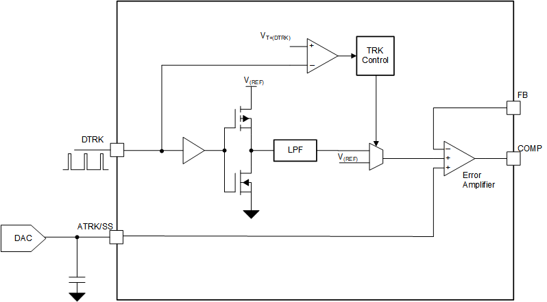
There are two kinds of output voltage tracking features integrated in the device.
- Analog voltage tracking function through the SS/ATRK pin
- Digital voltage tracking function through the DTRK pin
Analog Voltage Tracking
For the analog output voltage tracking, an external applied voltage overwrites the reference voltage for the output regulation loop. Although it is possible, it is not recommended to apply this voltage before the soft start is finished because the soft-start ramp time and, therefore, the input current during the start-up is changed.
As the internal error amplifier is designed to use the lowest reference input voltage, the applied voltage on the SS/ATRK pin is only effective for voltages lower than the Vref of the feedback pin. Hence, the maximum voltage for the output is determined by the resistor network on the FB pin.
If the analog voltage tracking is used to start-up the converter voltage a change at the mode pin from high to low or low to high will indicate the logic that the soft-start is completed.
Digital Voltage Tracking
The DTRK input of the LM5177 directly modulates the internal reference voltage. This function activates if the voltage on the DTRK pin is higher than the rising threshold of VT(DTRK) and a PWM signal in the recommended frequency is applied to the pin.
The maximum output voltage during digital tracking cannot exceed the nominal reference voltage for the FB resistor divider. The applied PWM signal reduces the internal reference voltage in relation with the duty cycle on the DTRK pin. A small duty cycle means less output voltage and a high duty cycle of the PWM input represents a high output voltage. For example, a duty cycle of 30% causes a output voltage of 30% of the selected voltage by the FB divider resistors.
 Figure 7-15 Output Voltage Tracking
Functional Block Diagram