SNVSBU4E June 2022 – August 2024 LM5177
PRODUCTION DATA
- 1
- 1 Features
- 2 Applications
- 3 Description
- 4 Pin Configuration and Functions
- 5 Specifications
- 6 Parameter Measurement Information
-
7 Detailed Description
- 7.1 Overview
- 7.2 Functional Block Diagram
- 7.3
Feature Description
- 7.3.1 Power-On Reset (POR System)
- 7.3.2 Buck-Boost Control Scheme
- 7.3.3 Power Save Mode
- 7.3.4 Supply Voltage Selection – VMAX Switch
- 7.3.5 Enable and Undervoltage Lockout
- 7.3.6 Oscillator Frequency Selection
- 7.3.7 Frequency Synchronization
- 7.3.8 Voltage Regulation Loop
- 7.3.9 Output Voltage Tracking
- 7.3.10 Slope Compensation
- 7.3.11 Configurable Soft Start
- 7.3.12 Peak Current Sensor
- 7.3.13 Current Monitoring and Current Limit Control Loop
- 7.3.14 Short Circuit - Hiccup Protection
- 7.3.15 nFLT Pin and Protections
- 7.3.16 Device Configuration Pin
- 7.3.17 Dual Random Spread Spectrum – DRSS
- 7.3.18 Gate Driver
- 7.4 Device Functional Modes
-
8 Application and Implementation
- 8.1 Application Information
- 8.2
Typical Application
- 8.2.1 Design Requirements
- 8.2.2
Detailed Design Procedure
- 8.2.2.1 Custom Design with WEBENCH Tools
- 8.2.2.2 Frequency
- 8.2.2.3 Feedback Divider
- 8.2.2.4 Inductor and Current Sense Resistor Selection
- 8.2.2.5 Slope Compensation
- 8.2.2.6 Output Capacitor
- 8.2.2.7 Input Capacitor
- 8.2.2.8 UVLO Divider
- 8.2.2.9 Soft-Start Capacitor
- 8.2.2.10 MOSFETs QH1 and QL1
- 8.2.2.11 MOSFETs QH2 and QL2
- 8.2.2.12 Frequency Compensation
- 8.2.2.13 External Component Selection
- 8.2.3 Application Curves
- 8.3 System Examples
- 9 Power Supply Recommendations
- 10Layout
- 11Device and Documentation Support
- 12Revision History
- 13Mechanical, Packaging, and Orderable Information
Package Options
Mechanical Data (Package|Pins)
- DCP|38
Thermal pad, mechanical data (Package|Pins)
- DCP|38
Orderable Information
3 Description
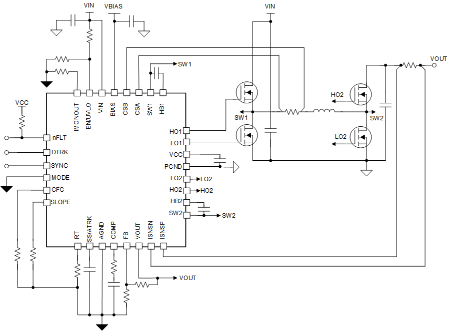
The LM5177 is a four switch buck-boost controller. The device provides a regulated output voltage if the input voltage is higher, equal, or lower than the adjusted output voltage. In power save mode, the device supports high efficiency with low output loads due to its low quiescence currents. The LM5177 runs at a fixed switching frequency, which can be set through the RT or SYNC pin. The switching frequency remains the same during buck, boost, and buck-boost operation. The integrated and optional average current monitor can help monitor and limit input and output current of the LM5177. This feature also supports charging backup power elements, like batteries or capacitors, with constant current (CC) and constant voltage (CV).
| Part Number | Package(1) | Body Size (NOM) |
|---|---|---|
| LM5177 | DCP038 | 9.7 mm × 4.4 mm |

Efficiency vs Input Voltage (IO = 4.5 A)

Simplified Schematic