SNVSBU4F June 2022 – January 2025 LM5177
PRODUCTION DATA
- 1
- 1 Features
- 2 Applications
- 3 Description
- 4 Pin Configuration and Functions
- 5 Specifications
- 6 Parameter Measurement Information
-
7 Detailed Description
- 7.1 Overview
- 7.2 Functional Block Diagram
- 7.3
Feature Description
- 7.3.1 Power-On Reset (POR System)
- 7.3.2 Buck-Boost Control Scheme
- 7.3.3 Power Save Mode
- 7.3.4 Supply Voltage Selection – VMAX Switch
- 7.3.5 Enable and Undervoltage Lockout
- 7.3.6 Oscillator Frequency Selection
- 7.3.7 Frequency Synchronization
- 7.3.8 Voltage Regulation Loop
- 7.3.9 Output Voltage Tracking
- 7.3.10 Slope Compensation
- 7.3.11 Configurable Soft Start
- 7.3.12 Peak Current Sensor
- 7.3.13 Current Monitoring and Current Limit Control Loop
- 7.3.14 Short Circuit - Hiccup Protection
- 7.3.15 nFLT Pin and Protections
- 7.3.16 Device Configuration Pin
- 7.3.17 Dual Random Spread Spectrum – DRSS
- 7.3.18 Gate Driver
- 7.4 Device Functional Modes
-
8 Application and Implementation
- 8.1 Application Information
- 8.2
Typical Application
- 8.2.1 Design Requirements
- 8.2.2
Detailed Design Procedure
- 8.2.2.1 Custom Design with WEBENCH Tools
- 8.2.2.2 Frequency
- 8.2.2.3 Feedback Divider
- 8.2.2.4 Inductor and Current Sense Resistor Selection
- 8.2.2.5 Slope Compensation
- 8.2.2.6 Output Capacitor
- 8.2.2.7 Input Capacitor
- 8.2.2.8 UVLO Divider
- 8.2.2.9 Soft-Start Capacitor
- 8.2.2.10 MOSFETs QH1 and QL1
- 8.2.2.11 MOSFETs QH2 and QL2
- 8.2.2.12 Frequency Compensation
- 8.2.2.13 External Component Selection
- 8.2.3 Application Curves
- 9 Power Supply Recommendations
- 10Layout
- 11Device and Documentation Support
- 12Revision History
- 13Mechanical, Packaging, and Orderable Information
Package Options
Mechanical Data (Package|Pins)
- DCP|38
Thermal pad, mechanical data (Package|Pins)
- DCP|38
Orderable Information
7.3.8 Voltage Regulation Loop
The LM5177 features an internal error amplifier (EA) to regulate the output voltage. The output voltage gets sensed on the FB pin through external resistors, which determine the target or nominal output voltage. The reference for the EA builds the soft-start and analog output voltage tracking pin (SS/ATRK). The COMP pin is the output of the internal gm-stage and gets connected to the external compensation network. The voltage over the compensation network is the nominal value for the inner peak current control loop of the device.
.
Use the following equations to calculate the external components:
External Feedback:
For most applications, TI recommends the following guidelines for bandwidth selection of the compensation.
The hard limit of the bandwidth (f(BW)) is the right half plane zero of the boost operation:
The maximum recommended bandwidth must be within the following boundaries:
The compensation zero (fCZ) must be placed in relation to the dominating pole of the boost.
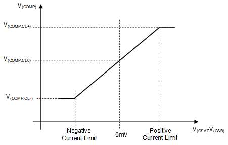
Due to the precise implementation of the error amplifier, the voltage on the LM5177 COMP pin is accurately reflecting the nominal peak current value of the inductor. Figure 7-13 shows the control V/I-characteristics of the error amplifier in FPWM mode. Use this as a guidance for applicative designs where you need to manipulate the inner current loop regulation.

Figure 7-13 Control Function for the Peak Current Sense Voltage Versus VCOMP