SNVSBU4E June 2022 – August 2024 LM5177
PRODUCTION DATA
- 1
- 1 Features
- 2 Applications
- 3 Description
- 4 Pin Configuration and Functions
- 5 Specifications
- 6 Parameter Measurement Information
-
7 Detailed Description
- 7.1 Overview
- 7.2 Functional Block Diagram
- 7.3
Feature Description
- 7.3.1 Power-On Reset (POR System)
- 7.3.2 Buck-Boost Control Scheme
- 7.3.3 Power Save Mode
- 7.3.4 Supply Voltage Selection – VMAX Switch
- 7.3.5 Enable and Undervoltage Lockout
- 7.3.6 Oscillator Frequency Selection
- 7.3.7 Frequency Synchronization
- 7.3.8 Voltage Regulation Loop
- 7.3.9 Output Voltage Tracking
- 7.3.10 Slope Compensation
- 7.3.11 Configurable Soft Start
- 7.3.12 Peak Current Sensor
- 7.3.13 Current Monitoring and Current Limit Control Loop
- 7.3.14 Short Circuit - Hiccup Protection
- 7.3.15 nFLT Pin and Protections
- 7.3.16 Device Configuration Pin
- 7.3.17 Dual Random Spread Spectrum – DRSS
- 7.3.18 Gate Driver
- 7.4 Device Functional Modes
-
8 Application and Implementation
- 8.1 Application Information
- 8.2
Typical Application
- 8.2.1 Design Requirements
- 8.2.2
Detailed Design Procedure
- 8.2.2.1 Custom Design with WEBENCH Tools
- 8.2.2.2 Frequency
- 8.2.2.3 Feedback Divider
- 8.2.2.4 Inductor and Current Sense Resistor Selection
- 8.2.2.5 Slope Compensation
- 8.2.2.6 Output Capacitor
- 8.2.2.7 Input Capacitor
- 8.2.2.8 UVLO Divider
- 8.2.2.9 Soft-Start Capacitor
- 8.2.2.10 MOSFETs QH1 and QL1
- 8.2.2.11 MOSFETs QH2 and QL2
- 8.2.2.12 Frequency Compensation
- 8.2.2.13 External Component Selection
- 8.2.3 Application Curves
- 8.3 System Examples
- 9 Power Supply Recommendations
- 10Layout
- 11Device and Documentation Support
- 12Revision History
- 13Mechanical, Packaging, and Orderable Information
Package Options
Mechanical Data (Package|Pins)
- DCP|38
Thermal pad, mechanical data (Package|Pins)
- DCP|38
Orderable Information
7.3.2 Buck-Boost Control Scheme
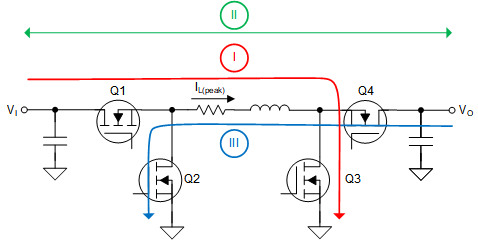
The LM5177 buck-boost control algorithm makes sure there is a seamless transition between the different operation modes, the fixed frequency operation, and the power stage protection features. The internal state machines controls the flowing three active switching states:
State I: Transistor Q1 and Q3 are conducting. Q2 and Q4 are not conducting (boost mode magnetization state).
State II: Transistor Q1 and Q4 are conducting. Q2 and Q3 are not conducting (boost demagnetization or buck magnetization state).
State III: Transistor Q2 and Q4 are conducting. Q1 and Q3 are not conducting (buck demagnetization state).
| Switch | State I | State II | State III |
|---|---|---|---|
| Q1 | ON | ON | OFF |
| Q2 | OFF | OFF | ON |
| Q3 | ON | OFF | OFF |
| Q4 | OFF | ON | ON |

Figure 7-1 Buck-Boost Active Switching States