SNVSC22B October 2023 – June 2024 LM51772
PRODUCTION DATA
- 1
- 1 Features
- 2 Applications
- 3 Description
- 4 Pin Configuration and Functions
- 5 Specifications
- 6 Parameter Measurement Information
-
7 Detailed Description
- 7.1 Overview
- 7.2 Functional Block Diagram
- 7.3
Feature Description
- 7.3.1 Buck-Boost Control Scheme
- 7.3.2 Power Save Mode
- 7.3.3 Programmable Conduction Mode PCM
- 7.3.4 Reference System
- 7.3.5 Supply Voltage Selection – VSMART Switch and Selection Logic
- 7.3.6 Enable and Undervoltage Lockout
- 7.3.7 Internal VCC Regulators
- 7.3.8 Error Amplifier and Control
- 7.3.9 Output Voltage Discharge
- 7.3.10 Peak Current Sensor
- 7.3.11 Short Circuit - Hiccup Protection
- 7.3.12 Current Monitor/Limiter
- 7.3.13 Oscillator Frequency Selection
- 7.3.14 Frequency Synchronization
- 7.3.15 Output Voltage Tracking
- 7.3.16 Slope Compensation
- 7.3.17 Configurable Soft Start
- 7.3.18 Drive Pin
- 7.3.19 Dual Random Spread Spectrum – DRSS
- 7.3.20 Gate Driver
- 7.3.21 Cable Drop Compensation (CDC)
- 7.3.22 CFG-pin and R2D Interface
- 7.3.23 Advanced Monitoring Features
- 7.3.24
Protection Features
- 7.3.24.1 Thermal Shutdown (TSD)
- 7.3.24.2 Over Current Protection
- 7.3.24.3 Output Over Voltage Protection 1 (OVP1)
- 7.3.24.4 Output Over Voltage Protection 2 (OVP2)
- 7.3.24.5 Input Voltage Protection (IVP)
- 7.3.24.6 Input Voltage Regulation (IVR)
- 7.3.24.7 Power Good
- 7.3.24.8 Boot-Strap Under Voltage Protection
- 7.3.24.9 Boot-strap Over Voltage Clamp
- 7.3.24.10 CRC - CHECK
- 7.4 Device Functional Modes
- 7.5 Programming
- 8 LM51772 Registers
-
9 Application and Implementation
- 9.1 Application Information
- 9.2
Typical Application
- 9.2.1 Design Requirements
- 9.2.2
Detailed Design Procedure
- 9.2.2.1 Custom Design with WEBENCH Tools
- 9.2.2.2 Frequency
- 9.2.2.3 Feedback Divider
- 9.2.2.4 Inductor and Current Sense Resistor Selection
- 9.2.2.5 Output Capacitor
- 9.2.2.6 Input Capacitor
- 9.2.2.7 Slope Compensation
- 9.2.2.8 UVLO Divider
- 9.2.2.9 Soft-Start Capacitor
- 9.2.2.10 MOSFETs QH1 and QL1
- 9.2.2.11 MOSFETs QH2 and QL2
- 9.2.2.12 Loop Compensation
- 9.2.2.13 External Component Selection
- 9.2.3 Application Curves
- 9.3 Power Supply Recommendations
- 9.4 Layout
- 9.5 USB-PD Source with Power Path
- 9.6 Parallel (Multiphase) Operation
- 9.7 Constant Current LED Driver
- 9.8 Wireless Charging Supply
- 9.9 Bi-Directional Power Backup
- 10Device and Documentation Support
- 11Revision History
- 12Mechanical, Packaging, and Orderable Information
Package Options
Mechanical Data (Package|Pins)
- RHA|40
Thermal pad, mechanical data (Package|Pins)
- RHA|40
Orderable Information
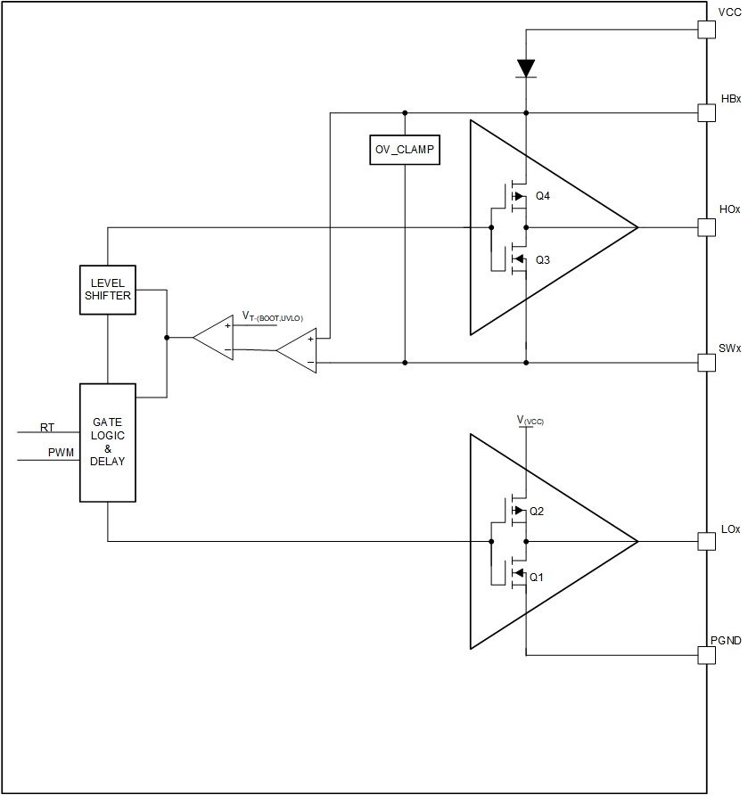
7.3.20 Gate Driver
The LM51772 features four internal logic-level nMOS gate drivers. The drivers maintain the high frequency switching of both half bridges needed for a buck-boost operation. If the device is in boost or buck mode, the other half bridge high-side switch needs to be permanent on. The internal gate drivers support this by sharing the current from the other half bridge, which is switching. Therefore, a minimum of quiescent current can be provided as no additional char pump is needed. Due to the high drive current capability, the LM51772 can support a wide range of external power FETs as well as a parallel operation of them.
The LO and HO outputs are protected with a shoot-through protection, which prevents both outputs to be turned on at the same time. If the PWM modulation logic of the buck-boost turns the LOx pin off, the HOx pin is not turned on until the following are true:
- A minimum internal transition time (tt(dead)) is reached.
- The voltage on the LOx pin drops below the detection threshold VTH(GATEOUT).
The high-side supply voltage for the gate driver are monitored by an additional bootstrap UVLO comparator. This comparator monitors the differential voltage between SWx and HBx. If the voltage drops below the threshold the buck-boost converter operation turns off. The device restarts automatically once the positive going threshold is reached with the soft-start scheme.
Additionally, the LM51772 monitors the upper voltage between SWx and HBx. If this voltage exceeds the threshold voltage of the clamping circuit, the LM51772 activates a internal current source to pull the voltage down.
The dead-time values can be controlled by SEL_SCALE_DT, SEL_MIN_DEADTIME_GDRV in the register Table 8-16.
The SEL_SCALE_DT can also be selected via the CFG-PIN (Table 7-6) in case the I2C interface is not used in the application. If enabled it increase the default dead time seeting by typically 15ns.
Additionally there is a optional frequency dependency of the transition (dead) -time between high and low side. This addresses the usual differences of the silicon MOSFET Qg in high power applications with low switching frequencies and lower power application with higher switching frequencies. When this option is enabled, the dead-time will be shorter when the switching frequency is set higher. The frequency dependency can be enabled or disabled with the register EN_CONST_TDEAD in register Table 8-16

Figure 7-31 Functional Block Diagram Gate Driver