SNVSC22B October 2023 – June 2024 LM51772
PRODUCTION DATA
- 1
- 1 Features
- 2 Applications
- 3 Description
- 4 Pin Configuration and Functions
- 5 Specifications
- 6 Parameter Measurement Information
-
7 Detailed Description
- 7.1 Overview
- 7.2 Functional Block Diagram
- 7.3
Feature Description
- 7.3.1 Buck-Boost Control Scheme
- 7.3.2 Power Save Mode
- 7.3.3 Programmable Conduction Mode PCM
- 7.3.4 Reference System
- 7.3.5 Supply Voltage Selection – VSMART Switch and Selection Logic
- 7.3.6 Enable and Undervoltage Lockout
- 7.3.7 Internal VCC Regulators
- 7.3.8 Error Amplifier and Control
- 7.3.9 Output Voltage Discharge
- 7.3.10 Peak Current Sensor
- 7.3.11 Short Circuit - Hiccup Protection
- 7.3.12 Current Monitor/Limiter
- 7.3.13 Oscillator Frequency Selection
- 7.3.14 Frequency Synchronization
- 7.3.15 Output Voltage Tracking
- 7.3.16 Slope Compensation
- 7.3.17 Configurable Soft Start
- 7.3.18 Drive Pin
- 7.3.19 Dual Random Spread Spectrum – DRSS
- 7.3.20 Gate Driver
- 7.3.21 Cable Drop Compensation (CDC)
- 7.3.22 CFG-pin and R2D Interface
- 7.3.23 Advanced Monitoring Features
- 7.3.24
Protection Features
- 7.3.24.1 Thermal Shutdown (TSD)
- 7.3.24.2 Over Current Protection
- 7.3.24.3 Output Over Voltage Protection 1 (OVP1)
- 7.3.24.4 Output Over Voltage Protection 2 (OVP2)
- 7.3.24.5 Input Voltage Protection (IVP)
- 7.3.24.6 Input Voltage Regulation (IVR)
- 7.3.24.7 Power Good
- 7.3.24.8 Boot-Strap Under Voltage Protection
- 7.3.24.9 Boot-strap Over Voltage Clamp
- 7.3.24.10 CRC - CHECK
- 7.4 Device Functional Modes
- 7.5 Programming
- 8 LM51772 Registers
-
9 Application and Implementation
- 9.1 Application Information
- 9.2
Typical Application
- 9.2.1 Design Requirements
- 9.2.2
Detailed Design Procedure
- 9.2.2.1 Custom Design with WEBENCH Tools
- 9.2.2.2 Frequency
- 9.2.2.3 Feedback Divider
- 9.2.2.4 Inductor and Current Sense Resistor Selection
- 9.2.2.5 Output Capacitor
- 9.2.2.6 Input Capacitor
- 9.2.2.7 Slope Compensation
- 9.2.2.8 UVLO Divider
- 9.2.2.9 Soft-Start Capacitor
- 9.2.2.10 MOSFETs QH1 and QL1
- 9.2.2.11 MOSFETs QH2 and QL2
- 9.2.2.12 Loop Compensation
- 9.2.2.13 External Component Selection
- 9.2.3 Application Curves
- 9.3 Power Supply Recommendations
- 9.4 Layout
- 9.5 USB-PD Source with Power Path
- 9.6 Parallel (Multiphase) Operation
- 9.7 Constant Current LED Driver
- 9.8 Wireless Charging Supply
- 9.9 Bi-Directional Power Backup
- 10Device and Documentation Support
- 11Revision History
- 12Mechanical, Packaging, and Orderable Information
Package Options
Mechanical Data (Package|Pins)
- RHA|40
Thermal pad, mechanical data (Package|Pins)
- RHA|40
Orderable Information
7.3.24.4 Output Over Voltage Protection 2 (OVP2)
This feature shall avoid any damage to the device in case the ext. feedback pin or compensatoin pin is not working properly (e.g. in case of a component or pin short)
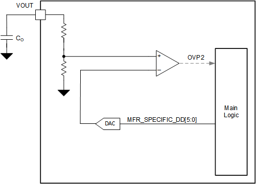
The over voltage protection is realized by the converter core and reference system. The absolute output voltage is monitored and when the OVP2 function is triggered the converter logic will take an appropriate measure (e.g. emergency skip mode) to avoid a further increase of the output voltage.
If the output voltage threshold VT+(OVP2) is reach on the VOUT-pin the buck-boost core logic disables the converter power stage and enters a high impedance state at the switch nodes. If the output voltage falls back under this threshold the converter operation is resumed
In order to accommodate a wide operating range, the OVP2 threshold is programmable by the V_OVP2 register field.
For power savings the OVP2 circuit can be turned off.

Figure 7-34 Functional Block Diagram OVP2