SNVSAW8E March 2020 – April 2022 LM62440-Q1
PRODUCTION DATA
- 1 Features
- 2 Applications
- 3 Description
- 4 Revision History
- 5 Description (continued)
- 6 Device Comparison Table
- 7 Pin Configuration and Functions
- 8 Specifications
-
9 Detailed Description
- 9.1 Overview
- 9.2 Functional Block Diagram
- 9.3
Feature Description
- 9.3.1 EN Uses for Enable and VIN UVLO
- 9.3.2 MODE/SYNC Pin Operation
- 9.3.3 PGOOD Output Operation
- 9.3.4 Internal LDO, VCC UVLO, and BIAS Input
- 9.3.5 Bootstrap Voltage and VCBOOT-UVLO (CBOOT Pin)
- 9.3.6 Adjustable SW Node Slew Rate
- 9.3.7 Spread Spectrum
- 9.3.8 Soft Start and Recovery From Dropout
- 9.3.9 Output Voltage Setting
- 9.3.10 Overcurrent and Short Circuit Protection
- 9.3.11 Thermal Shutdown
- 9.3.12 Input Supply Current
- 9.4 Device Functional Modes
-
10Application and Implementation
- 10.1 Application Information
- 10.2
Typical Application
- 10.2.1 Design Requirements
- 10.2.2
Detailed Design Procedure
- 10.2.2.1 Choosing the Switching Frequency
- 10.2.2.2 Setting the Output Voltage
- 10.2.2.3 Inductor Selection
- 10.2.2.4 Output Capacitor Selection
- 10.2.2.5 Input Capacitor Selection
- 10.2.2.6 BOOT Capacitor
- 10.2.2.7 BOOT Resistor
- 10.2.2.8 VCC
- 10.2.2.9 BIAS
- 10.2.2.10 CFF and RFF Selection
- 10.2.2.11 External UVLO
- 10.2.3 Application Curves
- 11Power Supply Recommendations
- 12Layout
- 13Device and Documentation Support
- 14Mechanical, Packaging, and Orderable Information
Package Options
Mechanical Data (Package|Pins)
- RJR|14
Thermal pad, mechanical data (Package|Pins)
Orderable Information
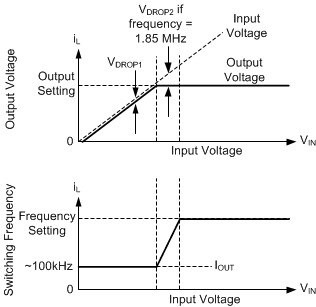
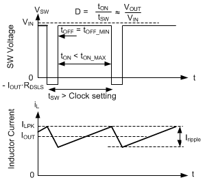
9.4.3.5 Dropout
Dropout operation is defined as any input-to-output voltage ratio that requires frequency to drop to achieve the required duty cycle. At a given clock frequency, duty cycle is limited by minimum off time. Once this limit is reached, if clock frequency were maintained, output voltage would fall. Instead of allowing the output voltage to drop, the LM62440-Q1 extends on time past the end of the clock cycle until the required peak inductor current is achieved. The clock is allowed to start a new cycle once peak inductor current is achieved or once a pre-determined maximum on time, tON_MAX, of approximately 9 µs passes. As a result, once the needed duty cycle cannot be achieved at the selected clock frequency due to the existence of a minimum off time, frequency drops to maintain regulation. If input voltage is low enough so that output voltage cannot be regulated even with an on time of tON_MAX, output voltage drops to slightly below the input voltage, VDROP1. For additional information on recovery from dropout, reference Figure 9-16.

