SNVSCH2 September 2024 LM65645-Q1
ADVANCE INFORMATION
- 1
- 1 Features
- 2 Applications
- 3 Description
- 4 Device Comparison Table
- 5 Pin Configuration and Functions
- 6 Specifications
-
7 Detailed Description
- 7.1 Overview
- 7.2 Functional Block Diagram
- 7.3
Feature Descriptions
- 7.3.1 Output Voltage Selection
- 7.3.2 EN Pin and Use as VIN UVLO
- 7.3.3 Mode Selection
- 7.3.4 Adjustable Switching Frequency
- 7.3.5 Dual Random Spread Spectrum (DRSS)
- 7.3.6 Internal LDO, VCC UVLO, and BIAS Input
- 7.3.7 Bootstrap Voltage (BST Pin)
- 7.3.8 Soft Start and Recovery From Dropout
- 7.3.9 Safety Features
- 7.4 Device Functional Modes
-
8 Application and Implementation
- 8.1 Application Information
- 8.2
Typical Application
- 8.2.1 Design Requirements
- 8.2.2
Detailed Design Procedure
- 8.2.2.1 Custom Design With WEBENCH® Tools
- 8.2.2.2 Choosing the Switching Frequency
- 8.2.2.3 FB for Adjustable or Fixed Output Voltage Mode
- 8.2.2.4 Inductor Selection
- 8.2.2.5 Output Capacitor Selection
- 8.2.2.6 Input Capacitor Selection
- 8.2.2.7 CBOOT
- 8.2.2.8 External UVLO
- 8.2.2.9 Maximum Ambient Temperature
- 8.3 Best Design Practices
- 8.4 Power Supply Recommendations
- 8.5 Layout
- 9 Device and Documentation Support
- 10Revision History
- 11Mechanical, Packaging, and Orderable Information
Package Options
Mechanical Data (Package|Pins)
- RZT|20
Thermal pad, mechanical data (Package|Pins)
Orderable Information
7.4.2.3 FPWM Mode Operation
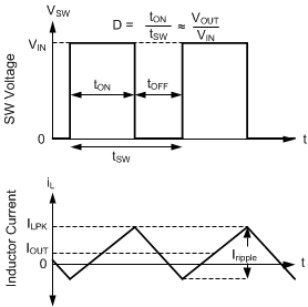
Like auto mode operation, FPWM mode operation during light-load operation is selected using the SYNC/MODE pin.
In FPWM Mode, frequency is maintained while lightly loaded. To maintain frequency, a limited reverse current is allowed to flow through the inductor. Reverse current is limited by reverse current limit circuitry. See the Electrical Characteristics for reverse current limit values.

In FPWM mode, frequency reduction is still available if output voltage is high enough to command minimum on-time, even while lightly loaded. This allows good behavior during faults which involves the output being pulled up.