SNIS194 December 2016 LM73-Q1
PRODUCTION DATA.
- 1 Features
- 2 Applications
- 3 Description
- 4 Revision History
- 5 Pin Configuration and Functions
- 6 Specifications
- 7 Detailed Description
- 8 Application and Implementation
- 9 Power Supply Recommendations
- 10Layout
- 11Device and Documentation Support
- 12Mechanical, Packaging, and Orderable Information
Package Options
Mechanical Data (Package|Pins)
- DDC|6
Thermal pad, mechanical data (Package|Pins)
Orderable Information
6 Specifications
6.1 Absolute Maximum Ratings
over operating free-air temperature range (unless otherwise noted)(1)(2)| MIN | NOM | MAX | UNIT | ||
|---|---|---|---|---|---|
| Supply Voltage | −0.3 | V to 6 | V | ||
| Voltage at SMBCLK and SMBDAT pins | −0.3 V to V | 6 | V | ||
| Voltage at All Other Pins | −0.3 | (VDD + 0.5) | 6 | V | |
| Input Current at Any Pin(1) | ±5 | mA | |||
| Storage Temperature, Tstg | −65 | 150 | °C | ||
(1) Stresses beyond those listed under Absolute Maximum Ratings may cause permanent damage to the device. These are stress ratings only, which do not imply functional operation of the device at these or any other conditions beyond those indicated under Recommended Operating Conditions. Exposure to absolute-maximum-rated conditions for extended periods may affect device reliability.
(2) Soldering process must comply with Texas Instruments' Reflow Temperature Profile specifications. Refer to www.ti.com/packaging.. Reflow temperature profiles are different for lead-free and non-lead-free packages.
6.2 ESD Ratings
| VALUE | UNIT | |||
|---|---|---|---|---|
| V(ESD) | Electrostatic discharge | Human-body model (HBM), per AEC Q100-002(1) | ±2000 | V |
| Charged-device model (CDM), per AEC Q100-011 | ±1000 | |||
(1) AEC Q100-002 indicates that HBM stressing shall be in accordance with the ANSI/ESDA/JEDEC JS-001 specification.
6.3 Recommended Operating Conditions
over operating free-air temperature range (unless otherwise noted)| MIN | MAX | UNIT | ||
|---|---|---|---|---|
| LM73-Q1 | –40 | 125 | °C | |
| Supply Voltage Range (VDD) | 2.7 | 5.5 | V | |
6.4 Thermal Information
| THERMAL METRIC(1) | LM73-Q1 | UNIT | |
|---|---|---|---|
| DDC (SOT) | |||
| 6 PINS | |||
| RθJA | Junction-to-ambient thermal resistance | 117 | °C/W |
| RθJC(top) | Junction-to-case (top) thermal resistance | 55 | |
| RθJA | Junction-to-board thermal resistance | 25 | |
| ψJT | Junction-to-top characterization parameter | 1 | |
| ψJB | Junction-to-board characterization parameter | 21 | |
(1) For more information about traditional and new thermal metrics, see the Semiconductor and IC Package Thermal Metrics application report.
6.5 Temperature-to-Digital Converter Characteristics
Unless otherwise noted, these specifications apply for VDD = 2.7 V to 5.5 V. All limits TA = TJ = 25°C, unless otherwise noted. TA is the ambient temperature. TJ is the junction temperature.| PARAMETER | TEST CONDITIONS | MIN | TYP | MAX | UNIT | ||
|---|---|---|---|---|---|---|---|
| Accuracy (2) | VDD = 3.3V | TA = −40°C to -25°C | –1.85 | 1.85 | °C | ||
| TA = −25°C to –10°C | –1.65 | 1.65 | °C | ||||
| TA = −10°C to 80°C | –1.45 | 1.45 | °C | ||||
| TA = 80°C to 115°C | –1.65 | 1.65 | °C | ||||
| TA = 115°C to 125°C | -1.8 | 1.8 | °C | ||||
| VDD = 2.7V to VDD = 4.5V |
TA = −40°C to -25°C | -2.1 | 2.1 | °C | |||
| TA = −25°C to –10°C | –1.75 | 1.75 | °C | ||||
| TA = −10°C to 80°C | -1.65 | 1.65 | °C | ||||
| TA = 80°C to 115°C | -1.8 | 1.8 | °C | ||||
| TA = 115°C to 125°C | -2 | 2 | °C | ||||
| VDD > 4.5V to VDD = 5.5V |
TA = −40°C to -25°C | -2.4 | 2.4 | °C | |||
| TA = −25°C to -10°C | -2.2 | 2.2 | °C | ||||
| TA = −10°C to 80°C | –1.9 | 1.9 | °C | ||||
| TA = 80°C to 115°C | -1.8 | 1.8 | °C | ||||
| TA = 115°C to 125°C | -2 | 2 | °C | ||||
| Resolution | RES1 Bit = 0, RES0 Bit = 0 | 11 | Bits | ||||
| 0.25 | °C/LSB | ||||||
| RES1 Bit = 0, RES0 Bit = 1 | 12 | Bits | |||||
| 0.125 | °C/LSB | ||||||
| RES1 Bit = 1, RES0 Bit = 0 | 13 | Bits | |||||
| 0.0625 | °C/LSB | ||||||
| RES1 Bit = 1, RES0 Bit = 1 | 14 | Bits | |||||
| 0.03125 | °C/LSB | ||||||
| Temperature Conversion Time (3) | RES1 Bit = 0, RES0 Bit = 0 | 10.1 | ms | ||||
| TA = TJ =TMIN to TMAX | 14 | ||||||
| RES1 Bit = 0, RES0 Bit = 1 | 20.2 | ms | |||||
| TA = TJ =TMIN to TMAX | 28 | ||||||
| RES1 Bit = 1, RES0 Bit = 0 | 40.4 | ms | |||||
| TA = TJ =TMIN to TMAX | 56 | ||||||
| RES1 Bit = 1, RES0 Bit = 1 | 80.8 | ms | |||||
| TA = TJ =TMIN to TMAX | 112 | ||||||
| Quiescent Current | Continuous Conversion Mode, SMBus inactive | 320 | µA | ||||
| TA = TJ =TMIN to TMAX | 495 | ||||||
| Shutdown, bus-idle timers on | 120 | µA | |||||
| TA = TJ =TMIN to TMAX | 175 | ||||||
| Shutdown, bus-idle timers off | 1.9 | µA | |||||
| TA = TJ =TMIN to TMAX | 8 | ||||||
| Power-On Reset Threshold | Measured on VDD input, falling edge | TA = TJ =TMIN to TMAX | 0.9 | V | |||
6.6 Logic Electrical Characteristics- Digital DC Characteristics
Unless otherwise noted, these specifications apply for VDD = 2.7 V to 5.5 V. All limits TA = TJ = 25°C, unless otherwise noted. TA is the ambient temperature. TJ is the junction temperature.| PARAMETER | TEST CONDITIONS | MIN | TYP | MAX | UNIT | ||
|---|---|---|---|---|---|---|---|
| SMBDAT, SMBCLK INPUTS | |||||||
| VIH | Logical 1 Input Voltage | TA = TJ =TMIN to TMAX | 0.7 × VDD | V | |||
| VIL | Logical 0 Input Voltage | TA = TJ =TMIN to TMAX | 0.3 × VDD | V | |||
| VIN;HYST | SMBDAT and SMBCLK Digital Input Hysteresis | 0.07 × VDD | V | ||||
| IIH | Logical 1 Input Current | VIN = VDD | 0.01 | µA | |||
| TA = TJ =TMIN to TMAX | 2 | ||||||
| IIL | Logical 0 Input Current | VIN = 0 V | –0.01 | µA | |||
| TA = TJ =TMIN to TMAX | –2 | ||||||
| CIN | Input Capacitance | 5 | pF | ||||
| SMBDAT, ALERT OUTPUTS | |||||||
| IOH | High Level Output Current | VOH = VDD | 0.01 | µA | |||
| TA = TJ =TMIN to TMAX | 2 | ||||||
| VOL | SMBus Low Level Output Voltage | IOL = 3 mA | TA = TJ =TMIN to TMAX | 0.4 | V | ||
| ADDRESS INPUT | |||||||
| VIH;ADDRESS | Address Pin High Input Voltage | TA = TJ =TMIN to TMAX | VDD – 0.100 | V | |||
| VIL;ADDRESS | Address Pin Low Input Voltage | TA = TJ =TMIN to TMAX | 0.100 | V | |||
| IIH; ADDRESS | Address Pin High Input Current | VIN = VDD | 0.01 | µA | |||
| TA = TJ =TMIN to TMAX | 2 | ||||||
| IIL;ADDRESS | Address Pin Low Input Current | VIN = 0 V | –0.01 | µA | |||
| TA = TJ =TMIN to TMAX | –2 | ||||||
6.7 SMBus Digital Switching Characteristics
Unless otherwise noted, these specifications apply for VDD = 2.7 V to 5.5 V, CL (load capacitance) on output lines = 400 pF. All limits TA = TJ = 25°C, unless otherwise noted. See Figure 1.| PARAMETER | TEST CONDITIONS | MIN | TYP | MAX | UNIT | ||
|---|---|---|---|---|---|---|---|
| fSMB | SMBus Clock Frequency | No minimum clock frequency if Time-Out feature is disabled. | TA = TJ =TMIN to TMAX | 400 | kHz | ||
| tLOW | SMBus Clock Low Time | TA = TJ =TMIN to TMAX | 300 | ns | |||
| tHIGH | SMBus Clock High Time | TA = TJ =TMIN to TMAX | 300 | ns | |||
| tF;SMBO | Output Fall Time (4) | CL = 400 pF IPULL-UP ≤ 3 mA |
TA = TJ =TMIN to TMAX | 250 | ns | ||
| tTIMEOUT | SMBDAT and SMBCLK Time Low for Reset of Serial Interface (5) | TA = TJ =TMIN to TMAX | 15 | 45 | ms | ||
| tSU;DAT | Data In Setup Time to SMBCLK High | TA = TJ =TMIN to TMAX | 100 | ns | |||
| tHD;DATI | Data Hold Time: Data In Stable after SMBCLK Low | TA = TJ =TMIN to TMAX | 0 | ns | |||
| tHD;DATO | Data Hold Time: Data Out Stable after SMBCLK Low | TA = TJ =TMIN to TMAX | 30 | ns | |||
| tHD;STA | Start Condition SMBDAT Low to SMBCLK Low (Start condition hold before the first clock falling edge) | TA = TJ =TMIN to TMAX | 60 | ns | |||
| tSU;STO | Stop Condition SMBCLK High to SMBDAT Low (Stop Condition Setup) | TA = TJ =TMIN to TMAX | 50 | ns | |||
| tSU;STA | SMBus Repeated Start-Condition Setup Time, SMBCLK High to SMBDAT Low | TA = TJ =TMIN to TMAX | 50 | ns | |||
| tBUF | SMBus Free Time Between Stop and Start Conditions | TA = TJ =TMIN to TMAX | 1.2 | µs | |||
| tPOR | Power-On Reset Time (6) | TA = TJ =TMIN to TMAX | 1 | ms | |||
(1) When the input voltage (VI) at any pin exceeds the power supplies (VI < GND or VI > VDD), the current at that pin should be limited to 5 mA.
(2) Local temperature accuracy does not include the effects of self-heating. The rise in temperature due to self-heating is the product of the internal power dissipation of the LM73-Q1 and the thermal resistance.
(3) This specification is provided only to indicate how often temperature data is updated. The LM73-Q1 can be read at any time without regard to conversion state (and will yield last conversion result).
(4) The output fall time is measured from (VIH;MIN + 0.15V) to (VIL;MAX - 0.15V).
(5) Holding the SMBDAT and/or SMBCLK lines Low for a time interval greater than tTIMEOUT will reset the LM73-Q1's SMBus state machine, setting SMBDAT and SMBCLK pins to a high impedance state.
(6) Represents the time from VDD reaching the power-on-reset level to the LM73-Q1 communications being functional. After an additional time equal to one temperature conversion time, valid temperature is available in the Temperature Data Register.
 Figure 1. SMBus Communication
6.8 Typical Characteristics
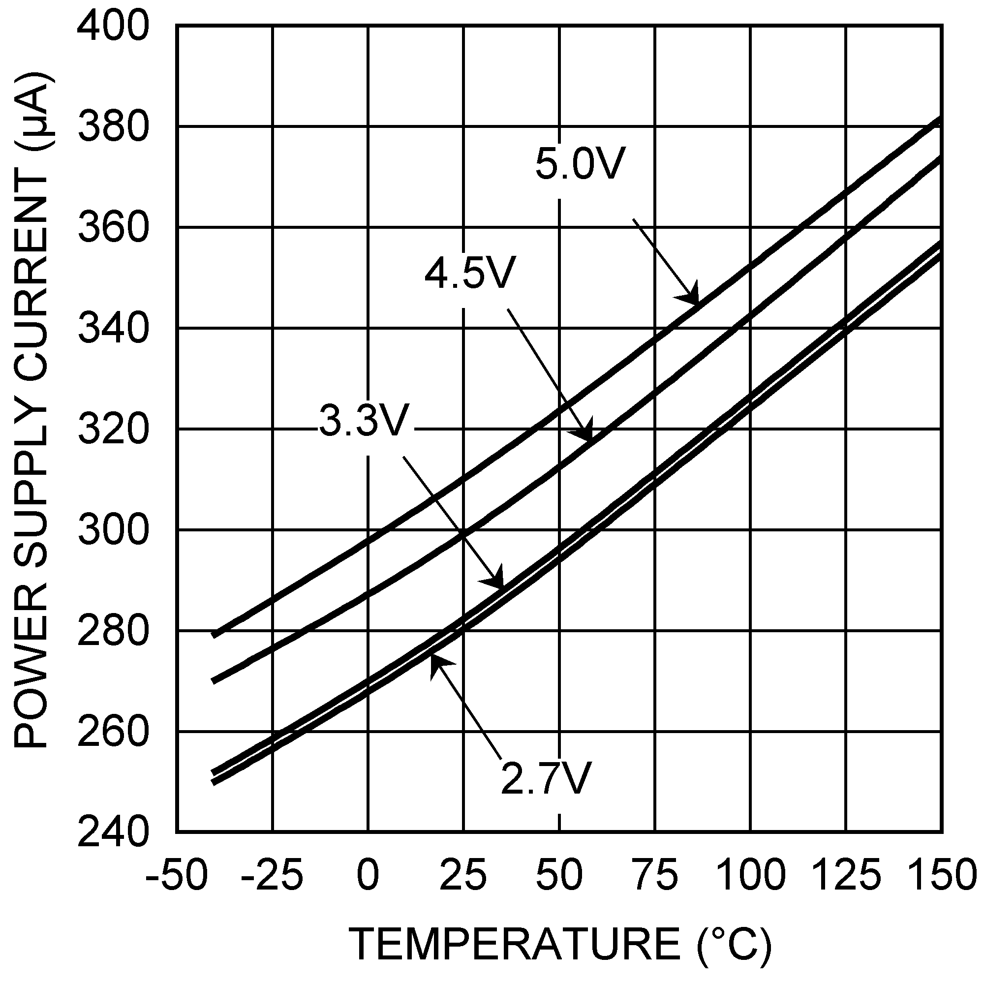
 Figure 2. Operating Current vs. Temperature
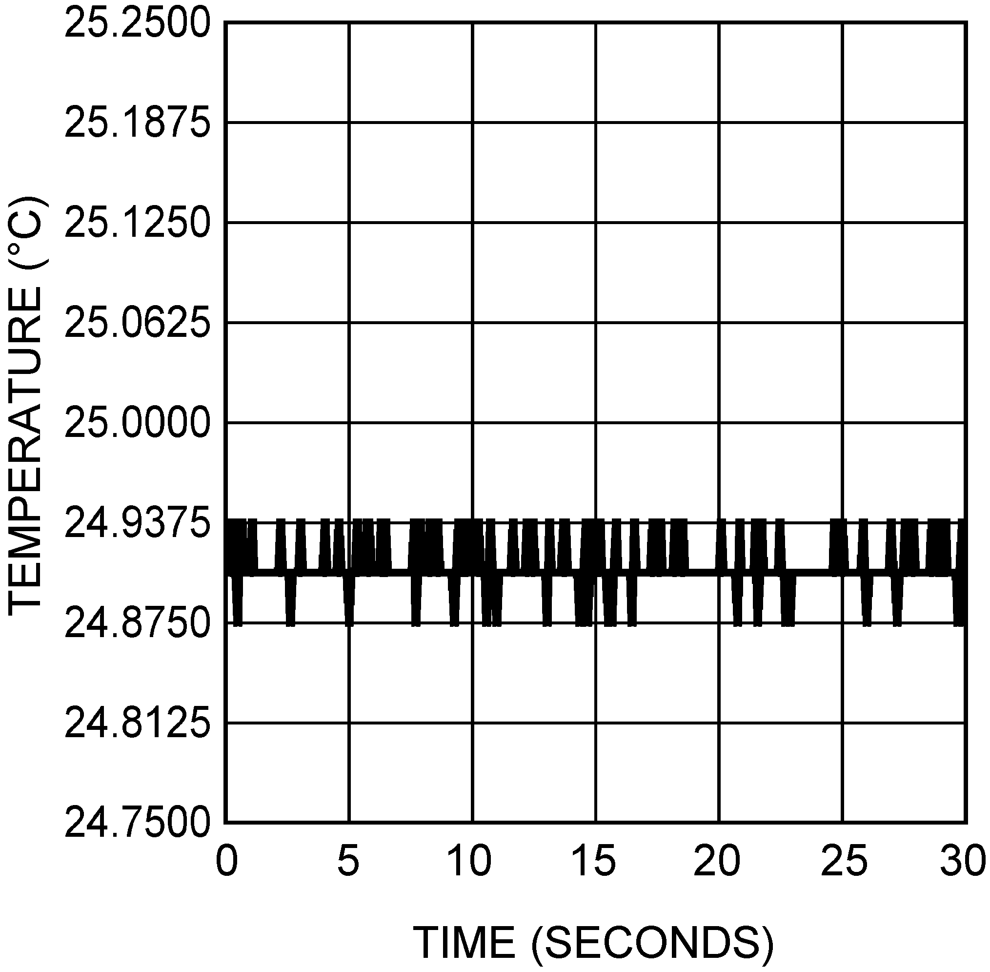
 Figure 4. Typical Output Noise
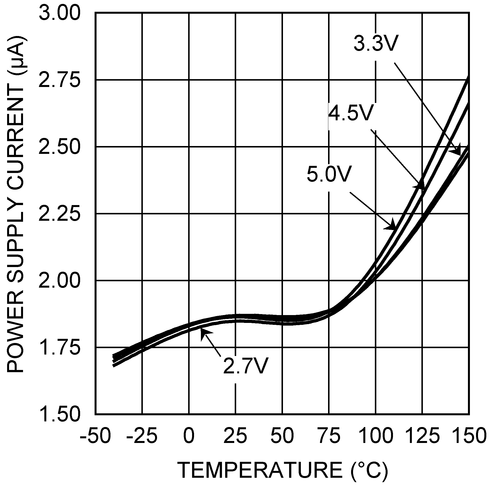
 Figure 3. Shutdown Current vs.Temperature