SNVSB12B November 2017 – May 2021 LM73605-Q1 , LM73606-Q1
PRODUCTION DATA
- 1 Features
- 2 Applications
- 3 Description
- 4 Revision History
- 5 Device Comparison
- 6 Pin Configuration and Functions
- 7 Specifications
-
8 Detailed Description
- 8.1 Overview
- 8.2 Functional Block Diagram
- 8.3
Feature Description
- 8.3.1 Synchronous Step-Down Regulator
- 8.3.2 Auto Mode and FPWM Mode
- 8.3.3 Fixed-Frequency Peak Current-Mode Control
- 8.3.4 Adjustable Output Voltage
- 8.3.5 Enable and UVLO
- 8.3.6 Internal LDO, VCC_UVLO, and BIAS Input
- 8.3.7 Soft Start and Voltage Tracking
- 8.3.8 Adjustable Switching Frequency
- 8.3.9 Frequency Synchronization and Mode Setting
- 8.3.10 Internal Compensation and CFF
- 8.3.11 Bootstrap Capacitor and VBOOT-UVLO
- 8.3.12 Power-Good and Overvoltage Protection
- 8.3.13 Overcurrent and Short-Circuit Protection
- 8.3.14 Thermal Shutdown
- 8.4 Device Functional Modes
- 9 Layout
- 10Device and Documentation Support
Package Options
Mechanical Data (Package|Pins)
- RNP|30
Thermal pad, mechanical data (Package|Pins)
- RNP|30
Orderable Information
7.9 Typical Characteristics
Unless otherwise specified, VIN = 12 V. Curves represent most likely parametric norm at specified condition.
 Figure 7-1 High-Side and Low-Side Switches RDS-ON
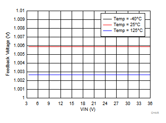
 Figure 7-3 Feedback Voltage
 Figure 7-5 LM73605-Q1 High-Side and Low-Side Current Limit
 Figure 7-7 Switching Frequency with RT Pin Open Circuit
 Figure 7-9 PGOOD Thresholds
 Figure 7-2 Shutdown Quiescent Current
 Figure 7-4 LM73605-Q1 High-Side and Low-Side Current Limits
 Figure 7-6 Switching Frequency Set by RT Resistor
 Figure 7-8 Enable Thresholds