SNVSBK6A February 2020 – July 2020 LM76005-Q1
PRODUCTION DATA
- 1 Features
- 2 Applications
- 3 Description
- 4 Revision History
- 5 Pin Configuration and Functions
- 6 Specifications
-
7 Detailed Description
- 7.1 Overview
- 7.2 Functional Block Diagram
- 7.3
Feature Description
- 7.3.1 Fixed-Frequency, Peak-Current-Mode Control
- 7.3.2 Light Load Operation Modes — PFM and FPWM
- 7.3.3 Adjustable Output Voltage
- 7.3.4 Enable (EN Pin) and UVLO
- 7.3.5 Internal LDO, VCC UVLO, and Bias Input
- 7.3.6 Soft Start and Voltage Tracking (SS/TRK)
- 7.3.7 Adjustable Switching Frequency (RT) and Frequency Synchronization
- 7.3.8 Minimum On-Time, Minimum Off-Time, and Frequency Foldback at Dropout Conditions
- 7.3.9 Bootstrap Voltage and VBOOT UVLO (BOOT Pin)
- 7.3.10 Power Good and Overvoltage Protection (PGOOD)
- 7.3.11 Overcurrent and Short-Circuit Protection
- 7.3.12 Thermal Shutdown
- 7.4 Device Functional Modes
-
8 Application and Implementation
- 8.1 Application Information
- 8.2
Typical Applications
- 8.2.1 Design Requirements
- 8.2.2
Detailed Design Procedure
- 8.2.2.1 Custom Design With WEBENCH® Tools
- 8.2.2.2 Output Voltage Setpoint
- 8.2.2.3 Switching Frequency
- 8.2.2.4 Input Capacitors
- 8.2.2.5 Inductor Selection
- 8.2.2.6 Output Capacitor Selection
- 8.2.2.7 Feedforward Capacitor
- 8.2.2.8 Bootstrap Capacitors
- 8.2.2.9 VCC Capacitors
- 8.2.2.10 BIAS Capacitors
- 8.2.2.11 Soft-Start Capacitors
- 8.2.2.12 Undervoltage Lockout Setpoint
- 8.2.2.13 PGOOD
- 8.2.2.14 Synchronization
- 8.2.3 Application Curves
- 9 Power Supply Recommendations
- 10Layout
- 11Device and Documentation Support
- 12Mechanical, Packaging, and Orderable Information
Package Options
Mechanical Data (Package|Pins)
- RNP|30
Thermal pad, mechanical data (Package|Pins)
- RNP|30
Orderable Information
3 Description
The LM76005-Q1 regulator is an easy-to-use synchronous step-down DC-DC converter capable of driving up to 5 A (LM76005-Q1) of load current from an input up to 60 V. Tolerance goes up to 65 V, easing input surge protection.
The LM76005-Q1 use peak-current-mode control to provide exceptional efficiency and output accuracy in a small solution size. Seamless transition between PWM and PFM modes, along with very low MOSFET ON resistances and an external bias input, ensures exceptional efficiency across the entire load range.
This device requires few external components and has a pinout designed for simple PCB layout with best-in-class EMI (CISPR25) and thermal performance. The small solution size and feature set of the LM76005-Q1 are designed to simplify the implementation for a wide range of end equipment.
The LM76005-Q1 device is available in the WQFN 30-pin leadless package with wettable flanks.
| PART NUMBER (1) | PACKAGE | BODY SIZE (NOM) |
|---|---|---|
| LM76005-Q1 | WQFN (30) | 6.00 mm × 4.00 mm |
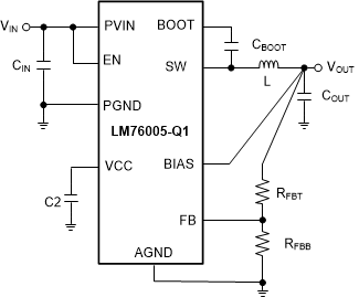
 Simplified Schematic
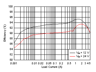
 Efficiency: VOUT = 5 V, fSW = 400 kHz, Auto Mode