SNVS233C March 2003 – December 2015 LM8365
PRODUCTION DATA.
- 1 Features
- 2 Applications
- 3 Description
- 4 Revision History
- 5 Pin Configuration and Functions
- 6 Specifications
- 7 Detailed Description
- 8 Application and Implementation
- 9 Power Supply Recommendations
- 10Layout
- 11Device and Documentation Support
- 12Mechanical, Packaging, and Orderable Information
Package Options
Mechanical Data (Package|Pins)
- DBV|5
Thermal pad, mechanical data (Package|Pins)
Orderable Information
8 Application and Implementation
NOTE
Information in the following applications sections is not part of the TI component specification, and TI does not warrant its accuracy or completeness. TI’s customers are responsible for determining suitability of components for their purposes. Customers should validate and test their design implementation to confirm system functionality.
8.1 Application Information
The LM8365 is a supervisor that is ideal for use in battery powered microprocessor based systems. With an external delay capacitor, CD, a time delay can be accurately programmed to allow for use in many types of applications. The LM8365 can ensure system reliability and ensures that a connected microprocessor will operate only when a minimum VIN supply is satisfied.
8.2 Typical Application
The LM8365 can be used as a simple supervisor circuit to monitor the input supply to a microprocessor as shown in Figure 14.
 Figure 14. Microprocessor Reset Circuit
8.2.1 Design Requirements
For this design example, use the parameters listed in Table 1 as the input parameters.
Table 1. Design Parameters
| DESIGN PARAMETER | EXAMPLE VALUE |
|---|---|
| Input Supply voltage range | 1 V to 6 V |
| Reset Output voltage, high | Input Supply |
| Reset Output voltage, low | 0 V |
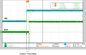
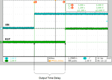
| Output Time delay, CD = 0.1 μF | 130 ms |
| Output Time delay, CD = 1 μF | 1.2 s |
8.2.2 Detailed Design Procedure
The Bill of Materials shown in Table 2 reflects the components used on the LM8365EVM. A layout of the EVM can be seen in Figure 19.
Table 2. Bill of Materials
| DESIGNATOR | DESCRIPTION | PART NUMBER | QUANTITY | MANUFACTURER |
|---|---|---|---|---|
| U1 | LM8365, 2.7V Threshold | LM8365 | 1 | Texas Instruments |
| R1 | 470K Resistor, 0603 | CRCW0603470KJNEA | 1 | Vishay |
| C1 | 0.01μF Capacitor, 0603 | GRM188R71C103KA01D | 1 | MuRata |
| C2 | 0.1μF Capacitor, 0805 | GRM219R71C104KA01D | 1 | MuRata |
| C3 | 1μF Capacitor, 0805 | C0805C105K4RACTU | 1 | Kemet |
| C4 | Input Capacitor | – | 0 | – |
8.3 System Examples
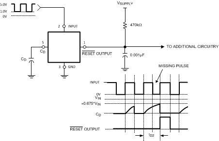
The LM8365 can be used as a missing pulse detector. As shown in Figure 17, if a high-to-low transition pulse were to be missing, the CD voltage would continue to increase until it reaches its threshold of 0.675 × VIN, causing the Reset pin to output high and signal a missing pulse.
 Figure 17. Missing Pulse Detector Using LM8365BALMF45

