SNOSDE2A October 2022 – December 2022 LMG2610
PRODUCTION DATA
- 1 Features
- 2 Applications
- 3 Description
- 4 Revision History
- 5 Pin Configuration and Functions
- 6 Specifications
- 7 Parameter Measurement Information
-
8 Detailed Description
- 8.1 Overview
- 8.2 Functional Block Diagram
- 8.3
Feature Description
- 8.3.1 GaN Power FET Switching Capability
- 8.3.2 Turn-On Slew-Rate Control
- 8.3.3 Current-Sense Emulation
- 8.3.4 Bootstrap Diode Function
- 8.3.5 Input Control Pins (EN, INL, INH)
- 8.3.6 INL - INH Interlock
- 8.3.7 AUX Supply Pin
- 8.3.8 BST Supply Pin
- 8.3.9 Over-Current Protection
- 8.3.10 Over-Temperature Protection
- 8.3.11 Fault Reporting
- 8.4 Device Functional Modes
- 9 Application and Implementation
- 10Device and Documentation Support
- 11Mechanical, Packaging, and Orderable Information
Package Options
Mechanical Data (Package|Pins)
- RRG|40
Thermal pad, mechanical data (Package|Pins)
Orderable Information
3 Description
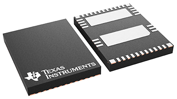
The LMG2610 is a 650-V GaN power-FET half bridge intended for < 75-W active-clamp flyback (ACF) converters in switch mode power supply applications. The LMG2610 simplifies design, reduces component count, and reduces board space by integrating half-bridge power FETs, gate drivers, bootstrap diode, and high-side gate-drive level shifter in a 9-mm by 7-mm QFN package.
The asymmetric GaN FET resistances are optimized for ACF operating conditions. Programmable turn-on slew rates provide EMI and ringing control. The low-side current-sense emulation reduces power dissipation compared to the traditional current-sense resistor and allows the low-side thermal pad to be connected to the cooling PCB power ground.
The high-side gate-drive signal level shifter eliminates noise and burst-mode power dissipation problems found with external solutions. The smart-switched GaN bootstrap FET has no diode forward-voltage drop, avoids overcharging the high-side supply, and has zero reverse-recovery charge.
The LMG2610 supports converter light-load efficiency requirements and burst-mode operation with low quiescent currents and fast start-up times. Protection features include FET turn-on interlock, under-voltage lockout (UVLO), cycle-by-cycle current limit, and over-temperature shut down.
| PART NUMBER | PACKAGE(1) | BODY SIZE (NOM) |
|---|---|---|
| LMG2610 | QFN | 9.00 mm x 7.00 mm |