SNOSDH5 November   2024 LMG2640

PRODUCTION DATA  

  1.   1
  2. Features
  3. Applications
  4. Description
  5. Pin Configuration and Functions
  6. Specifications
    1. 5.1 Absolute Maximum Ratings
    2. 5.2 ESD Ratings
    3. 5.3 Recommended Operating Conditions
    4. 5.4 Thermal Information
    5. 5.5 Electrical Characteristics
    6. 5.6 Switching Characteristics
    7. 5.7 Typical Characteristics
  7. Parameter Measurement Information
    1. 6.1 GaN Power FET Switching Parameters
  8. Detailed Description
    1. 7.1 Overview
    2. 7.2 Functional Block Diagram
    3. 7.3 Feature Description
      1. 7.3.1  GaN Power FET Switching Capability
      2. 7.3.2  Current-Sense Emulation
      3. 7.3.3  Bootstrap Diode Function
      4. 7.3.4  Input Control Pins (EN, INL, INH)
      5. 7.3.5  INL - INH Interlock
      6. 7.3.6  AUX Supply Pin
        1. 7.3.6.1 AUX Power-On Reset
        2. 7.3.6.2 AUX Under-Voltage Lockout (UVLO)
      7. 7.3.7  BST Supply Pin
        1. 7.3.7.1 BST Power-On Reset
        2. 7.3.7.2 BST Under-Voltage Lockout (UVLO)
      8. 7.3.8  Over-Current Protection
      9. 7.3.9  Over-Temperature Protection
      10. 7.3.10 Fault Reporting
    4. 7.4 Device Functional Modes
  9. Application and Implementation
    1. 8.1 Application Information
    2. 8.2 Typical Application
      1. 8.2.1 Design Requirements
      2. 8.2.2 Detailed Design Procedure
      3. 8.2.3 Application Curve
    3. 8.3 Power Supply Recommendations
    4. 8.4 Layout
      1. 8.4.1 Layout Guidelines
        1. 8.4.1.1 Solder-Joint Stress Relief
        2. 8.4.1.2 Signal-Ground Connection
        3. 8.4.1.3 CS Pin Signal
      2. 8.4.2 Layout Example
  10. Device and Documentation Support
    1. 9.1 Documentation Support
      1. 9.1.1 Related Documentation
    2. 9.2 Receiving Notification of Documentation Updates
    3. 9.3 Support Resources
    4. 9.4 Trademarks
    5. 9.5 Electrostatic Discharge Caution
    6. 9.6 Glossary
  11. 10Revision History
  12. 11Mechanical, Packaging, and Orderable Information

Package Options

Refer to the PDF data sheet for device specific package drawings

Mechanical Data (Package|Pins)
  • RRG|40
Thermal pad, mechanical data (Package|Pins)
Orderable Information

Description

The LMG2640 is a 650V GaN power-FET half bridge intended for switch mode power supply applications. The LMG2640 simplifies design, reduces component count, and reduces board space by integrating half-bridge power FETs, gate drivers, bootstrap diode, and high-side gate-drive level shifter in a 9mm by 7mm QFN package.

The low-side current-sense emulation reduces power dissipation compared to the traditional current-sense resistor and allows the low-side thermal pad to be connected to the cooling PCB power ground.

The high-side gate-drive signal level shifter eliminates noise and burst-mode power dissipation problems found with external solutions. The smart-switched GaN bootstrap FET has no diode forward-voltage drop, avoids overcharging the high-side supply, and has zero reverse-recovery charge.

The LMG2640 supports converter light-load efficiency requirements and burst-mode operation with low quiescent currents and fast start-up times. Protection features include FET turn-on interlock, under-voltage lockout (UVLO), cycle-by-cycle current limit, and over-temperature shut down.
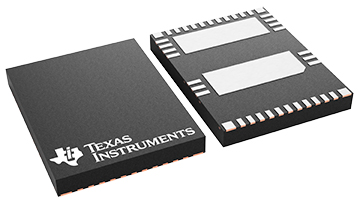
Package Information
PART NUMBER PACKAGE(1) PACKAGE SIZE(2)
LMG2640 RRG (QFN, 40) 9.00mm × 7.00mm
For more information, see the Section 11 section.
The package size (length × width) is a nominal value and includes pins, where applicable.
LMG2640 Package
          View Package View