SNOSD91B March   2019  – February 2020 LMG3410R150 , LMG3411R150

PRODUCTION DATA.  

  1. Features
  2. Applications
  3. Description
    1.     Device Images
      1.      Simplified Block Diagram
      2.      Switching Performance
  4. Revision History
  5. Pin Configuration and Functions
    1.     Pin Functions
  6. Specifications
    1. 6.1 Absolute Maximum Ratings
    2. 6.2 ESD Ratings
    3. 6.3 Recommended Operating Conditions
    4. 6.4 Thermal Information
    5. 6.5 Electrical Characteristics
    6. 6.6 Switching Characteristics
    7. 6.7 Typical Characteristics
  7. Parameter Measurement Information
    1. 7.1 Switching Parameters
    2. 7.2 Turn-on Delays
    3. 7.3 Turn-off Delays
    4. 7.4 Drain Slew Rate
  8. Detailed Description
    1. 8.1 Overview
    2. 8.2 Functional Block Diagram
    3. 8.3 Feature Description
      1. 8.3.1 Direct-Drive GaN Architecture
      2. 8.3.2 Internal Buck-Boost DC-DC Converter
      3. 8.3.3 Internal Auxiliary LDO
      4. 8.3.4 Start Up Sequence
      5. 8.3.5 R-C Decoupling for IN pin
      6. 8.3.6 Low Power Mode
      7. 8.3.7 Fault Detection
        1. 8.3.7.1 Overcurrent Protection
        2. 8.3.7.2 Over-Temperature Protection and UVLO
      8. 8.3.8 Drive Strength Adjustment
    4. 8.4 Safe Operation Area (SOA)
      1. 8.4.1 Repetitive SOA
  9. Application and Implementation
    1. 9.1 Application Information
    2. 9.2 Typical Application
      1. 9.2.1 Design Requirements
      2. 9.2.2 Detailed Design Procedure
        1. 9.2.2.1 Slew Rate Selection
          1. 9.2.2.1.1 Startup and Slew Rate with Bootstrap High-Side Supply
        2. 9.2.2.2 Signal Level-Shifting
        3. 9.2.2.3 Buck-Boost Converter Design
    3. 9.3 Dos and Don'ts
  10. 10Power Supply Recommendations
    1. 10.1 Using an Isolated Power Supply
    2. 10.2 Using a Bootstrap Diode
      1. 10.2.1 Diode Selection
      2. 10.2.2 Managing the Bootstrap Voltage
      3. 10.2.3 Reliable Bootstrap Start-up
  11. 11Layout
    1. 11.1 Layout Guidelines
      1. 11.1.1 Power Loop Inductance
      2. 11.1.2 Signal Ground Connection
      3. 11.1.3 Bypass Capacitors
      4. 11.1.4 Switch-Node Capacitance
      5. 11.1.5 Signal Integrity
      6. 11.1.6 High-Voltage Spacing
      7. 11.1.7 Thermal Recommendations
    2. 11.2 Layout Example
  12. 12Device and Documentation Support
    1. 12.1 Device Support
      1. 12.1.1 Third-Party Products Disclaimer
    2. 12.2 Documentation Support
      1. 12.2.1 Related Documentation
    3. 12.3 Receiving Notification of Documentation Updates
    4. 12.4 Community Resources
    5. 12.5 Trademarks
    6. 12.6 Electrostatic Discharge Caution
    7. 12.7 Glossary
  13. 13Mechanical, Packaging, and Orderable Information

Package Options

Mechanical Data (Package|Pins)
Thermal pad, mechanical data (Package|Pins)
Orderable Information

Low Power Mode

In some applications, it is important to reduce quiescent current during low power mode such as start up or burst. The LPM pin reduces the quiescent current to support low power modes. When LPM is pulled low, the buck-boost converter stops to operate and reduce additional power loss, and the supply current in the low-power mode is typically 80 µA. Figure 16 indicates the low power mode operation. Once it is activated, VNEG will recharge FAULT will become high. Only after the LPM deactivates, the buck-boost converter begins to build the VNEG, and LMG341xR150 begins to operate within 1 ms.
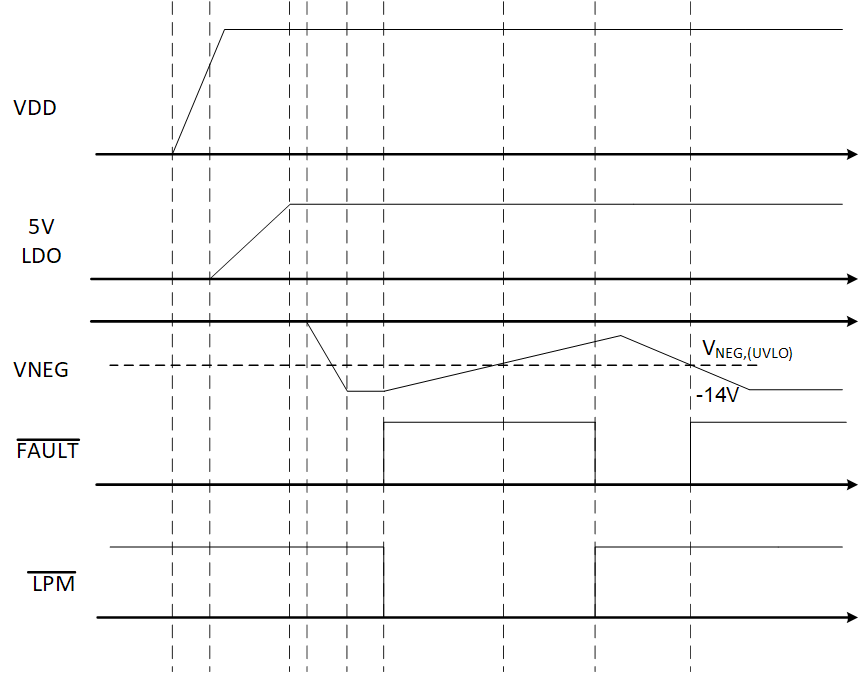
LMG3411R150 LMG3410R150 Timing-LPM.gifFigure 16. LPM in and out Timing Diagram