SNOSCY4E March 2015 – October 2018 LMG5200
PRODUCTION DATA.
- 1 Features
- 2 Applications
- 3 Description
- 4 Revision History
- 5 Pin Configuration and Functions
- 6 Specifications
- 7 Parameter Measurement Information
- 8 Detailed Description
- 9 Application and Implementation
- 10Power Supply Recommendations
- 11Layout
- 12Device and Documentation Support
- 13Mechanical, Packaging, and Orderable Information
Package Options
Mechanical Data (Package|Pins)
- MOF|9
Thermal pad, mechanical data (Package|Pins)
Orderable Information
7.1 Propagation Delay and Mismatch Measurement
Figure 5 shows the typical test setup used to measure the propagation mismatch. As the gate drives are not accessible, pullup and pulldown resistors in this test circuit are used to indicate when the low-side GaN FET turns ON and the high-side GaN FET turns OFF and vice versa to measure the tMON and tMOFF parameters. Resistance values used in this circuit for the pullup and pulldown resistors are in the order of 1 kΩ; the current sources used are 2 A.
Figure 6 through Figure 9 show propagation delay measurement waveforms. For turnon propagation delay measurements, the current sources are not used. For turnoff time measurements, the current sources are set to 2 A, and a voltage clamp limit is also set, referred to as VIN(CLAMP). When measuring the high-side component turnoff delay, the current source across the high-side FET is turned on, the current source across the low-side FET is off, HI transitions from high-to-low, and output voltage transitions from VIN to VIN(CLAMP). Similarly, for low-side component turnoff propagation delay measurements, the high-side component current source is turned off, and the low-side component current source is turned on, LI transitions from high to low and the output transitions from GND potential to VIN(CLAMP). The time between the transition of LI and the output change is the propagation delay time.
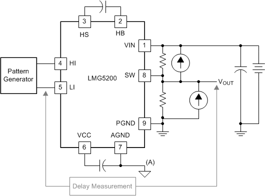 Figure 5. Propagation Delay and Propagation Mismatch Measurement
 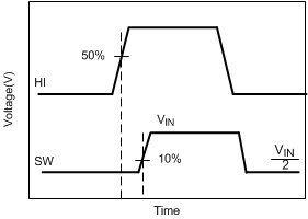 Figure 6. High-Side Gate Driver Turnon
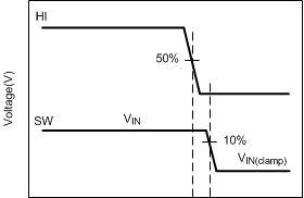
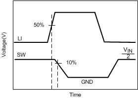 Figure 7. Low-Side Gate Driver Turnon
 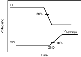 Figure 9. Low-Side Gate Driver Turnoff