SNLS474E February   2015  – June 2018 LMH1218

PRODUCTION DATA.  

  1. Features
  2. Applications
  3. Description
    1.     Device Images
      1.      Simplified SPI Schematic
  4. Revision History
  5. Pin Configuration and Functions
    1.     Pin Descriptions – SPI Mode/ Mode_SEL = 1 kΩ to VDD
    2.     Pin Descriptions – SMBUS Mode/ MODE_SEL = 1 kΩ to GND
  6. Specifications
    1. 6.1 Absolute Maximum Ratings
    2. 6.2 ESD Ratings
    3. 6.3 Recommended Operating Conditions
    4. 6.4 Thermal Information
    5. 6.5 Electrical Characteristics
    6. 6.6 Recommended SMBus Interface AC Timing Specifications
    7. 6.7 Serial Parallel Interface (SPI) Bus Interface AC Timing Specifications
    8. 6.8 Typical Characteristics
  7. Detailed Description
    1. 7.1 Overview
    2. 7.2 Functional Block Diagram
    3. 7.3 Feature Description
      1. 7.3.1 Loss of Signal Detector
      2. 7.3.2 Continuous Time Linear Equalizer (CTLE)
      3. 7.3.3 2:1 Multiplexer
      4. 7.3.4 Clock and Data Recovery
      5. 7.3.5 Eye Opening Monitor (EOM)
      6. 7.3.6 Fast EOM
        1. 7.3.6.1 SMBus Fast EOM Operation
        2. 7.3.6.2 SPI Fast EOM Operation
      7. 7.3.7 LMH1218 Device Configuration
        1. 7.3.7.1 MODE_SEL
        2. 7.3.7.2 ENABLE
        3. 7.3.7.3 LOS_INT_N
        4. 7.3.7.4 LOCK
        5. 7.3.7.5 SMBus MODE
        6. 7.3.7.6 SMBus READ/WRITE Transaction
        7. 7.3.7.7 SPI Mode
          1. 7.3.7.7.1 SPI READ/WRITE Transaction
          2. 7.3.7.7.2 SPI Write Transaction Format
          3. 7.3.7.7.3 SPI Read Transaction Format
        8. 7.3.7.8 SPI Daisy Chain
          1. 7.3.7.8.1 SPI Daisy Chain Write Example
          2. 7.3.7.8.2 SPI Daisy Chain Write Read Example
            1. 7.3.7.8.2.1 SPI Daisy Chain Length of Daisy Chain Illustration
      8. 7.3.8 Power-On Reset
    4. 7.4 Device Functional Modes
    5. 7.5 Programming
    6. 7.6 Register Maps
      1. 7.6.1 Global Registers
      2. 7.6.2 Receiver Registers
      3. 7.6.3 CDR Registers
      4. 7.6.4 Transmitter Registers
  8. Application and Implementation
    1. 8.1 Application Information
      1. 8.1.1 General Guidance for All Applications
    2. 8.2 Typical Application
      1. 8.2.1 Design Requirements
      2. 8.2.2 Detailed Design Procedure
      3. 8.2.3 Application Curves
    3. 8.3 Do's and Don'ts
    4. 8.4 Initialization Set Up
      1. 8.4.1 Selective Data Rate Lock
  9. Power Supply Recommendations
  10. 10Layout
    1. 10.1 Layout Guidelines
    2. 10.2 Layout Example
    3. 10.3 Solder Profile
  11. 11Device and Documentation Support
    1. 11.1 Device Support
      1. 11.1.1 Development Support
    2. 11.2 Documentation Support
      1. 11.2.1 Related Documentation
    3. 11.3 Receiving Notification of Documentation Updates
    4. 11.4 Community Resources
    5. 11.5 Trademarks
    6. 11.6 Electrostatic Discharge Caution
    7. 11.7 Glossary
  12. 12Mechanical, Packaging, and Orderable Information

Package Options

Mechanical Data (Package|Pins)
Thermal pad, mechanical data (Package|Pins)
Orderable Information

Typical Application

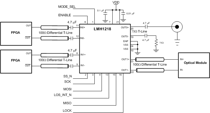
LMH1218 new_fig_25.gifFigure 23. LMH1218 SPI Mode Configuration

The LMH1218 has strong equalization capabilities that allow it to recover data over lossy channel up to 27 dB at 6 GHz. As a result, the optimal placement for the LMH1218 is with the higher loss channel at its input and lower loss channel segment at the output in order to meet the various SMPTE requirements. To meet SMPTE requirements, it is strongly recommended to put the LMH1218 as close as possible to the BNC (within 1 inch). The LMH1218 can be used as a cable driver with integrated reclocker or as reclocker only.