SBOSA33A September 2021 – December 2021 LMH5485-SP
ADVANCE INFORMATION
- 1 Features
- 2 Applications
- 3 Description
- 4 Revision History
- 5 Device Comparison Table
- 6 Pin Configuration and Functions
-
7 Specifications
- 7.1 Absolute Maximum Ratings
- 7.2 ESD Ratings
- 7.3 Recommended Operating Conditions
- 7.4 Thermal Information
- 7.5 Electrical Characteristics: VS+ – VS– = 5 V
- 7.6 Electrical Characteristics: VS+ – VS– = 3 V
- 7.7 Quality Conformance Inspection
- 7.8 Typical Characteristics: 5 V Single Supply
- 7.9 Typical Characteristics: 3 V Single Supply
- 7.10 Typical Characteristics: 3 V to 5 V Supply Range
- 8 Parameter Measurement Information
-
9 Detailed Description
- 9.1 Overview
- 9.2 Functional Block Diagram
- 9.3 Feature Description
- 9.4
Device Functional Modes
- 9.4.1
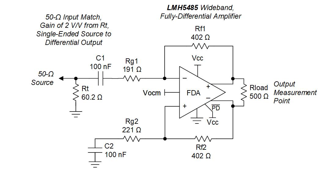
Operation from Single-Ended Sources to Differential Outputs
- 9.4.1.1 AC-Coupled Signal Path Considerations for Single-Ended Input to Differential Output Conversion
- 9.4.1.2 DC-Coupled Input Signal Path Considerations for Single-Ended to Differential Conversion
- 9.4.1.3 Resistor Design Equations for the Single-Ended to Differential Configuration of the FDA
- 9.4.1.4 Input Impedance for the Single-Ended to Differential FDA Configuration
- 9.4.2 Differential-Input to Differential-Output Operation
- 9.4.1
Operation from Single-Ended Sources to Differential Outputs
- 10Power Supply Recommendations
- 11Layout
- 12Device and Documentation Support
- 13Mechanical, Packaging, and Orderable Information
Package Options
Refer to the PDF data sheet for device specific package drawings
Mechanical Data (Package|Pins)
- HKX|8
Thermal pad, mechanical data (Package|Pins)
Orderable Information
3 Description
The LMH5485-SP is a radiation , low-power, voltage-feedback, fully differential amplifier (FDA) with an input common-mode range below the negative rail, and rail-to-rail output. Designed for power sensitive data acquisition systems where high density is critical in a high-performance analog-to-digital converter (ADC) or digital-to-analog converter (DAC) interface designs.
The LMH5485-SP features the negative-rail input required when interfacing a DC-coupled, ground-centered, source signal. This negative-rail input, with rail-to-rail output, allows for easy interface between single-ended, ground-referenced, bipolar signal sources and a wide variety of successive approximation register (SAR), delta-sigma (ΔΣ), or pipeline ADCs using only a single 2.7 V to 5.1 V power supply. LMH5485-SP also offers excellent DC precision for such ADC driving applications and is characterized for operation over the wide temperature range of –55°C to +125°C.
| PART NUMBER(1) | GRADE | PACKAGE |
|---|---|---|
| 5962R1920401VXC | Radiation hardness assured (RHA) | Ceramic CFP HKX (8) 6.5 mm × 6.5 mm |
| 5962-1920401VXC | QMLV | |
| LMH5485HKX/EM | Engineering samples(2) |
 Simplified
Schematic