SNOSAL8D April 2006 – September 2021 LMH6321
PRODUCTION DATA
- 1Features
- 2Applications
- 3Description
- 4Revision History
- 5Specifications
- 6Application Hints
- 7Device and Documentation Support
- 8Mechanical, Packaging, and Orderable Information
Package Options
Refer to the PDF data sheet for device specific package drawings
Mechanical Data (Package|Pins)
- KTW|7
- DDA|8
Thermal pad, mechanical data (Package|Pins)
Orderable Information
6.10 Single Supply Operation
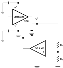
If dual supplies are used, then the GND pin can be connected to a hard ground (0 V) (as shown in Figure 6-2). However, if only a single supply is used, this pin must be set to a voltage of one VBE (≈0.7 V) or greater, or more commonly, mid rail, by a stiff, low impedance source. This precludes applying a resistive voltage divider to the GND pin for this purpose. Figure 6-6 shows one way that this can be done.
 Figure 6-6 Using an Op Amp to Bias the GND Pin to ½ V+ for Single Supply Operation
In Figure 6-6, the op amp circuit pre-biases the GND pin of the buffer for single supply operation.
The GND pin can be driven by an op amp configured as a constant voltage source, with the output voltage set by the resistor voltage divider, R1 and R2. It is recommended that These resistors be chosen so as to set the GND pin to V+/2, for maximum common mode range.