SNAS801B June   2020  – June 2021 LMK05318B

PRODUCTION DATA  

  1. Features
  2. Applications
  3. Description
  4. Revision History
  5. Description (continued)
  6. Pin Configuration and Functions
    1. 6.1 Device Start-Up Modes
  7. Specifications
    1. 7.1 Absolute Maximum Ratings
    2. 7.2 ESD Ratings
    3. 7.3 Recommended Operating Conditions
    4. 7.4 Thermal Information: 4-Layer JEDEC Standard PCB
    5. 7.5 Thermal Information: 10-Layer Custom PCB
    6. 7.6 Electrical Characteristics
    7. 7.7 Timing Diagrams
    8. 7.8 Typical Characteristics
  8. Parameter Measurement Information
    1. 8.1 Output Clock Test Configurations
  9. Detailed Description
    1. 9.1 Overview
      1. 9.1.1 ITU-T G.8262 (SyncE) Standards Compliance
    2. 9.2 Functional Block Diagram
      1. 9.2.1 PLL Architecture Overview
      2. 9.2.2 DPLL Mode
      3. 9.2.3 APLL-Only Mode
    3. 9.3 Feature Description
      1. 9.3.1  Oscillator Input (XO_P/N)
      2. 9.3.2  Reference Inputs (PRIREF_P/N and SECREF_P/N)
        1. 9.3.2.1 Programmable Input Hysteresis
      3. 9.3.3  Clock Input Interfacing and Termination
      4. 9.3.4  Reference Input Mux Selection
        1. 9.3.4.1 Automatic Input Selection
        2. 9.3.4.2 Manual Input Selection
      5. 9.3.5  Hitless Switching
        1. 9.3.5.1 Hitless Switching With 1-PPS Inputs
      6. 9.3.6  Gapped Clock Support on Reference Inputs
      7. 9.3.7  Input Clock and PLL Monitoring, Status, and Interrupts
        1. 9.3.7.1 XO Input Monitoring
        2. 9.3.7.2 Reference Input Monitoring
          1. 9.3.7.2.1 Reference Validation Timer
          2. 9.3.7.2.2 Amplitude Monitor
          3. 9.3.7.2.3 Frequency Monitoring
          4. 9.3.7.2.4 Missing Pulse Monitor (Late Detect)
          5. 9.3.7.2.5 Runt Pulse Monitor (Early Detect)
          6. 9.3.7.2.6 Phase Valid Monitor for 1-PPS Inputs
        3. 9.3.7.3 PLL Lock Detectors
        4. 9.3.7.4 Tuning Word History
        5. 9.3.7.5 Status Outputs
        6. 9.3.7.6 Interrupt
      8. 9.3.8  PLL Relationships
        1. 9.3.8.1  PLL Frequency Relationships
        2. 9.3.8.2  Analog PLLs (APLL1, APLL2)
        3. 9.3.8.3  APLL Reference Paths
          1. 9.3.8.3.1 APLL XO Doubler
          2. 9.3.8.3.2 APLL1 XO Reference (R) Divider
          3. 9.3.8.3.3 APLL2 Reference (R) Dividers
        4. 9.3.8.4  APLL Phase Frequency Detector (PFD) and Charge Pump
        5. 9.3.8.5  APLL Feedback Divider Paths
          1. 9.3.8.5.1 APLL1 N Divider With SDM
          2. 9.3.8.5.2 APLL2 N Divider With SDM
        6. 9.3.8.6  APLL Loop Filters (LF1, LF2)
        7. 9.3.8.7  APLL Voltage Controlled Oscillators (VCO1, VCO2)
          1. 9.3.8.7.1 VCO Calibration
        8. 9.3.8.8  APLL VCO Clock Distribution Paths (P1, P2)
        9. 9.3.8.9  DPLL Reference (R) Divider Paths
        10. 9.3.8.10 DPLL Time-to-Digital Converter (TDC)
        11. 9.3.8.11 DPLL Loop Filter (DLF)
        12. 9.3.8.12 DPLL Feedback (FB) Divider Path
      9. 9.3.9  Output Clock Distribution
      10. 9.3.10 Output Channel Muxes
      11. 9.3.11 Output Dividers (OD)
      12. 9.3.12 Clock Outputs (OUTx_P/N)
        1. 9.3.12.1 AC-Differential Output (AC-DIFF)
        2. 9.3.12.2 HCSL Output
        3. 9.3.12.3 1.8-V LVCMOS Output
        4. 9.3.12.4 Output Auto-Mute During LOL
      13. 9.3.13 Glitchless Output Clock Start-Up
      14. 9.3.14 Clock Output Interfacing and Termination
      15. 9.3.15 Output Synchronization (SYNC)
      16. 9.3.16 Zero-Delay Mode (ZDM) Synchronization for 1-PPS Input and Output
    4. 9.4 Device Functional Modes
      1. 9.4.1 Device Start-Up Modes
        1. 9.4.1.1 EEPROM Mode
        2. 9.4.1.2 ROM Mode
      2. 9.4.2 PLL Operating Modes
        1. 9.4.2.1 Free-Run Mode
        2. 9.4.2.2 Lock Acquisition
        3. 9.4.2.3 Locked Mode
        4. 9.4.2.4 Holdover Mode
      3. 9.4.3 PLL Start-Up Sequence
      4. 9.4.4 Digitally-Controlled Oscillator (DCO) Mode
        1. 9.4.4.1 DCO Frequency Step Size
        2. 9.4.4.2 DCO Direct-Write Mode
      5. 9.4.5 Zero-Delay Mode Synchronization
    5. 9.5 Programming
      1. 9.5.1 Interface and Control
      2. 9.5.2 I2C Serial Interface
        1. 9.5.2.1 I2C Block Register Transfers
      3. 9.5.3 SPI Serial Interface
        1. 9.5.3.1 SPI Block Register Transfer
      4. 9.5.4 Register Map and EEPROM Map Generation
      5. 9.5.5 General Register Programming Sequence
      6. 9.5.6 EEPROM Programming Flow
        1. 9.5.6.1 EEPROM Programming Using Method #1 (Register Commit)
          1. 9.5.6.1.1 Write SRAM Using Register Commit
          2. 9.5.6.1.2 Program EEPROM
        2. 9.5.6.2 EEPROM Programming Using Method #2 (Direct Writes)
          1. 9.5.6.2.1 Write SRAM Using Direct Writes
          2. 9.5.6.2.2 User-Programmable Fields In EEPROM
      7. 9.5.7 Read SRAM
      8. 9.5.8 Read EEPROM
      9. 9.5.9 EEPROM Start-Up Mode Default Configuration
  10. 10Application and Implementation
    1. 10.1 Application Information
      1. 10.1.1 Device Start-Up Sequence
      2. 10.1.2 Power Down (PDN) Pin
      3. 10.1.3 Power Rail Sequencing, Power Supply Ramp Rate, and Mixing Supply Domains
        1. 10.1.3.1 Mixing Supplies
        2. 10.1.3.2 Power-On Reset (POR) Circuit
        3. 10.1.3.3 Powering Up From a Single-Supply Rail
        4. 10.1.3.4 Power Up From Split-Supply Rails
        5. 10.1.3.5 Non-Monotonic or Slow Power-Up Supply Ramp
      4. 10.1.4 Slow or Delayed XO Start-Up
    2. 10.2 Typical Application
      1. 10.2.1 Design Requirements
      2. 10.2.2 Detailed Design Procedure
      3. 10.2.3 Application Curves
    3. 10.3 Do's and Don'ts
  11. 11Power Supply Recommendations
    1. 11.1 Power Supply Bypassing
    2. 11.2 Device Current and Power Consumption
      1. 11.2.1 Current Consumption Calculations
      2. 11.2.2 Power Consumption Calculations
      3. 11.2.3 Example
  12. 12Layout
    1. 12.1 Layout Guidelines
    2. 12.2 Layout Example
    3. 12.3 Thermal Reliability
      1. 12.3.1 Support for PCB Temperature up to 105 °C
  13. 13Device and Documentation Support
    1. 13.1 Device Support
      1. 13.1.1 TICS Pro
      2. 13.1.2 Related Documentation
    2. 13.2 Receiving Notification of Documentation Updates
    3. 13.3 Support Resources
    4. 13.4 Trademarks
    5. 13.5 Electrostatic Discharge Caution
    6. 13.6 Glossary
  14. 14Mechanical, Packaging, and Orderable Information

Package Options

Mechanical Data (Package|Pins)
Thermal pad, mechanical data (Package|Pins)
Orderable Information

Description (continued)

The DPLL supports programmable loop bandwidth for jitter and wander attenuation, while the two APLLs support fractional frequency translation for flexible clock generation. The synchronization options supported on the DPLL include hitless switching with phase cancellation, digital holdover, and DCO mode with less than 0.001-ppb (part per billion) frequency step size for precision clock steering (IEEE 1588 PTP slave). The DPLL can phase-lock to a 1-PPS (pulse-per-second) reference input and support optional zero-delay mode on one output to achieve deterministic input-to-output phase alignment with programmable offset. The advanced reference input monitoring block ensures robust clock fault detection and helps to minimize output clock disturbance when a loss of reference (LOR) occurs.

The device can use a commonly available low-frequency TCXO or OCXO to set the free-run or holdover output frequency stability per synchronization standards. Otherwise, the device can use a standard XO when free-run or holdover frequency stability and wander are not critical. The device is fully programmable through I2C or SPI interface, and supports custom frequency configuration on power up with the internal EEPROM or ROM. The EEPROM is factory pre-programmed and can be programmed in-system, if needed.
GUID-1876ADE7-1713-4E65-95B7-14ED532B3594-low.png
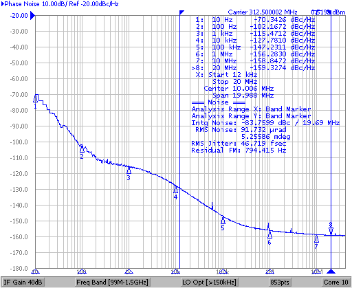
See Section 7.8 for Test Conditions.
Figure 5-1 312.5-MHz Output Phase Noise (APLL1), < 50-fs RMS Jitter