SNAS517E November 2011 – September 2015 LMP91050
PRODUCTION DATA.
- 1 Features
- 2 Applications
- 3 Description
- 4 Revision History
- 5 Description (continued)
- 6 Pin Configuration and Functions
- 7 Specifications
- 8 Detailed Description
- 9 Application and Implementation
- 10Power Supply Recommendations
- 11Layout
- 12Device and Documentation Support
- 13Mechanical, Packaging, and Orderable Information
Package Options
Mechanical Data (Package|Pins)
- DGS|10
Thermal pad, mechanical data (Package|Pins)
Orderable Information
8 Detailed Description
8.1 Overview
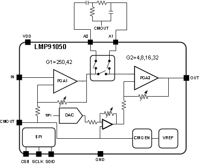
The input channel of the LMP91050 features two programmable gain stages that give the user flexibility in optimizing the system gain. Access to the inter-stage connection between the gain blocks also allows the inclusion of appropriate filtering if needed. The internal DAC allows the DC offset of the output voltage to be adjusted independently of the common-mode voltage supplied to the sensor, enabling the sampled signal to be centered within the ADC full-scale input range.
The following paragraphs discuss the LMP91050’s features in more detail.
8.2 Functional Block Diagram

8.3 Feature Description
8.3.1 Programmable Gain Amplifier
The LMP91050 offers two programmable gain modes (low or high) with four programmable gain settings each. The purpose of the gain mode is to enable thermopiles with larger dark voltage levels. All gain settings are accessible through bits GAIN1 and GAIN2[1:0]. The low-gain mode has a range of 167 V/V to 1335 V/V while the high-gain mode has a range of 1002 V/V to 7986 V/V. The PGA is referenced to the internally generated VCM. Input signal, referenced to this VCM voltage, should be within ±2 mV (see VINMAX_HGM specification) in high-gain mode. In the low gain mode the first stage will provide a gain of 42 V/V instead of 250 V/V, thus allowing a larger maximum input signal up to ±12 mV (VINMAX_LGM).
Table 1. Gain Modes
| BIT SYMBOL | GAIN |
|---|---|
| GAIN1 | 0: 250 (default) |
| 1: 42 | |
| GAIN2 [1:0] | 00: 4 (default) |
| 01: 8 | |
| 10: 16 | |
| 11: 32 |
8.3.2 External Filter
The LMP91050 offers two different measurement modes selectable through EXT_FILT bit. EXT_FILT bit is present in the Device configuration register and is programmable through SPI.
Table 2. Measurement Modes
| BIT SYMBOL | MEASUREMENT MODE |
|---|---|
| EXT_FILT | 0: The signal from the thermopile is being processed by the internal PGAs, without additional external decoupling or filtering (default). |
| 1: The signal from the thermopile is being processed by the first internal PGA and fed to the A0 pin. An external low pass, high pass or band pass filter can be connected through pins A0, A1. |
An external filter can be applied when EXT_FILT = 1. A typical band pass filter is shown in the picture below. Resistor and capacitor can be connected to the CMOUT pin of the LMP91050 as shown. Discrete component values have been added for reference.
 Figure 21. Typical Bandpass Filter
8.3.3 Offset Adjust
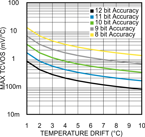
Procedure of the offset adjust is to first measure the dark signal, program the DAC to adjust, and then measure in a second cycle the residual of the dark signal for further signal manipulation within the µC. The signal source is expected to have an offset component (dark signal) larger than the actual signal. During the dark phase, the time when no light is detected by the sensor, the µC can program LMP91050 internal DAC to compensate for a measured offset. A low output offset voltage temperature drift (TCVOS) ensures system accuracy over temperature. See Figure 22 below which plots the maximum TCVOS allowed over a given temperature drift in order to achieve n bit system accuracy.
 Figure 22. System Accuracy vs. TCVOS and Temperature Drift
8.3.4 Common-Mode Generation
As the offset of the sensor is bipolar, there is a need to supply a VCM to the sensor. This can be programmed as 1.15 V or 2.59 V (approximately mid rail of 3.3-V or 5-V supply). TI does not recommend to use 2.59-V VCM with a 3.3-V supply
8.3.5 CSB
Chip Select is a active-low signal. CSB needs to be asserted throughout a transaction. That is, CSB should not pulse between the Instruction Byte and the Data Byte of a single transaction.
NOTE
CSB de-assertion always terminates an on-going transaction, if it is not already complete. Likewise, CSB assertion will always bring the device into a state, ready for next transaction, regardless of the termination status of a previous transaction.
CSB may be permanently tied low for a 2-wire SPI communication protocol.
8.3.5.1 SCLK
SCLK can idle High or Low for a write transaction. However, for a READ transaction, SCLK must idle high. SCLK features a Schmitt-triggered input and although it has hysterisis, TI recommends to keep SCLK as clean as possible to prevent glitches from inadvertently spoiling the SPI frame.
8.4 Device Functional Modes
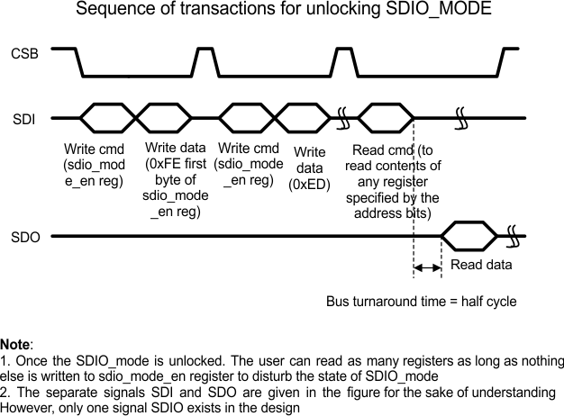
To read the registers of the LMP91050, the SDIO mode enable register must be written using a special sequence, as described in the SDIO Mode section. During the reading process, the analog OUT pin is still active, as normal. There are no other special modes for the device.
8.5 Programming
8.5.1 SPI Interface
An SPI interface is available in order to program the device parameters like PGA gain of two stages, enabling external filter, enabling power for PGAs, offset adjust and common-mode (VCM) voltage.
8.5.1.1 Interface Pins
The Serial Interface consists of SDIO (Serial Data Input / Output), SCLK (Serial Interface Clock) and CSB (Chip Select Bar). The serial interface is write-only by default. Read operations are supported after unlocking the SDIO_MODE_PASSWD. This is discussed in detail later in the document.
8.5.1.2 Communication Protocol
Communication on the SPI normally involves Write and Read transactions. Write transaction consists of single Write Command Byte, followed by single Data byte. The following figure shows the SPI Interface Protocol for write transaction.
 Figure 23. SPI Interface Protocol
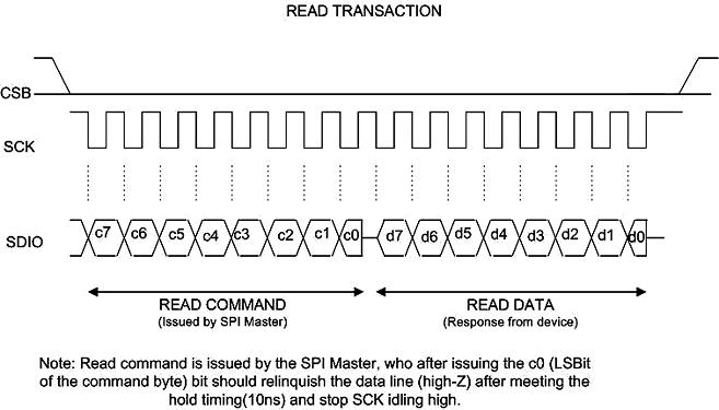
For Read transactions, user first needs to write into a SDIO mode enable register for enabling the SPI read mode. Once the device is enabled for Reading, the data is driven out on the SDIO pin during the Data field of the Read Transaction. SDIO pin is designed as a bidirectional pin for this purpose. Figure 24 shows the Read transaction. The sequence of commands that need to be issued by the SPI Master to enable SPI read mode is shown in Figure 25.
 Figure 24. Read Transaction
 Figure 25. Enable SDIO Mode for Reading SPI Registers
8.5.1.3 Registers Organization
Configuring the device is achieved using Write of the designated registers in the device. All the registers are organized into individually addressable byte-long registers that have a unique address. The format of the Write/ Read instruction is as shown below.
Table 3. Write / Read Instruction Format
| Bit[7] | Bit[6:4] | Bit[3:0] |
|---|---|---|
| 0 : Write Instruction | Reserved to 0 | Address |
| 1 : Read Instruction |
8.6 Register Maps
This section describes the programmable registers and the associated programming sequence, if any, for the device. Table 4 shows the summary listing of all the registers that are available to the user and their power-up values.
Table 4. Register Descriptions
| Title | Address (Hex) | Type | Power-up/Reset Value (Hex) |
|---|---|---|---|
| Device Configuration | 0x0 | Read-Write | 0x0 |
| (Read allowed in SDIO Mode) | |||
| DAC Configuration | 0x1 | Read-Write | 0x80 |
| (Read allowed in SDIO Mode) | |||
| SDIO Mode Enable | 0xF | Write-only | 0x0 |
8.6.1 Device Configuration
Table 5. Device Configuration Register (Address 0x0)
| Bit | Bit Symbol | Description |
|---|---|---|
| 7 | RESERVED | Reserved to 0. |
| [6:5] | EN | 00: PGA1 OFF PGA2 OFF (default) |
| 01: PGA1 OFF, PGA2 ON | ||
| 10: PGA1 ON, PGA2 OFF | ||
| 11: PGA1 ON, PGA2 ON | ||
| 4 | EXT_FILT | 0: PGA1 to PGA2 direct (default) |
| 1: PGA1 to PGA2 via external filter | ||
| 3 | CMN_MODE | 0 : 1.15V (default) |
| 1 : 2.59V | ||
| [2:1] | GAIN2 | 00: 4 (default) |
| 01: 8 | ||
| 10: 16 | ||
| 11: 32 | ||
| 0 | GAIN1 | 0: 250 (default) |
| 1: 42 |
8.6.2 DAC Configuration
The output DC level will shift according to the formula Vout_shift = -33.8mV * (NDAC - 128).
Table 6. DAC Configuration Register (Address 0x1)
| Bit | Bit Symbol | Description |
|---|---|---|
| [7:0] | NDAC | 128 (0x80): Vout_shift = -33.8mV * (128 - 128) = 0mV (default) |