LMP91300 Industrial Inductive Proximity Sensor AFE
1 Features
- Post Production Configuration and Calibration
- Programmable Decision Thresholds
- Programmable Hysteresis
- Flexible Overload Protection
- Digital Temperature Compensation
- Integrated LED driver
- Small Form Factor, Supports 4mm Sensors (DSBGA Package)
- Low Power Consumption
- Integrated Voltage Regulator
- 3-Wire Capability
- Supports NPN and PNP Modes
- Normally Open (NO) and Normally Closed (NC) Supported
- 16-bit Resolution Threshold Setting
2 Applications
- Industrial Proximity Detection
- Industrial Production Lines
- Industrial Automation
3 Description
The LMP91300 is a complete analog front end (AFE) optimized for use in industrial inductive proximity sensors. The LMP91300 directly converts the RP of the external LC tank into a digital value.
Post-manufacturing configuration and calibration is fully supported. The temperature dependence of the sensor is digitally compensated, using an external temperature sensor. The LMP91300 provides programmable thresholds, programmable temperature compensation and programmable oscillation frequency range. Due to its programmability, the LMP91300 can be used with a wide variety of external inductors and its detection thresholds can be adjusted to the desired detection distances.
An internal voltage regulator allows the device to operate with a supply from 6.5V to 40V. The output can be programmed to drive an external transistor in either NPN or PNP mode.
Available in 4mm × 5mm 24-terminal WQFN and 2.05mm × 2.67mm 20-terminal DSBGA packages, the LMP91300 operates from -40°C to +125°C.
Device Information
| ORDER NUMBER | PACKAGE | BODY SIZE |
|---|---|---|
| LMP91300NHZ | WQFN (24) | 4mm x 5mm |
| LMP91300YZR | DSBGA (20) | 2.05mm x 2.67mm |
4 Revision History
Changes from A Revision (September 2013) to B Revision
- Changed layout to new datasheet formatGo
- Added Burn Current Specification.Go
- Added additional information to Low RP, Close Target, Under Range Switch Enable section. Go
- Changed typo. Go
- Added additional information to REXTB section. Go
Changes from * Revision (September 2013) to A Revision
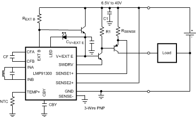
5 Terminal Configuration and Functions

LMP91300 WQFN Terminal Functions
| TERMINAL NUMBER | NAME | TYPE | DESCRIPTION |
|---|---|---|---|
| 1-5 | P1-5 | G | Connect to Ground |
| 6 | GND | G | Board Ground |
| 7 | LED | O | LED Driver Output |
| 8 | V+/EXT E | P | Chip V+/External transistor, emitter |
| 9 | EXT B | P | External transistor, base |
| 10 | SWDRV | O | Drive for external transistor switch |
| 11 | SENSE- | I | Negative sense Input |
| 12 | SENSE1+ | I | Positive sense Input |
| 13 | SENSE2+/SWIF RX | I | Positive sense Input and Single Wire Interface receive |
| 14 | NC | N/A | No connect |
| 15 | GND | G | Board ground |
| 16 | NC | N/A | No connect |
| 17 | CFB | I | Filter capacitor value based on sensor oscillation frequency |
| 18 | CFA | I | Filter capacitor value based on sensor oscillation frequency |
| 19 | GND | G | Board ground |
| 20 | INA | I | External LC tank |
| 21 | INB | I | External LC tank |
| 22 | TEMP- | G | NTC ground, connect to board ground |
| 23 | TEMP+ | I | Analog Temperature Sensor Input |
| 24 | CBY | O | Bypass capacitor (56nF) |
| DAP | DAP | G | Connect to Ground |

LMP91300 DSBGA Terminal Functions
| TERMINAL NUMBER | NAME | TYPE | DESCRIPTION |
|---|---|---|---|
| A1 | INA | I | External LC tank |
| A2 | INB | I | External LC tank |
| A3 | TEMP+ | I | Analog Temperature Sensor Input |
| A4 | CBY | O | Bypass capacitor (56nF) |
| B1 | CFA | I | Filter capacitor value based on sensor oscillation frequency |
| B2 | P2 | G | Connect to Ground |
| B3 | TEMP- | G | NTC ground, connect to board ground |
| B4 | P1 | G | Connect to Ground |
| C1 | CFB | I | Filter capacitor value based on sensor oscillation frequency |
| C2 | P5 | G | Connect to Ground |
| C3 | P4 | G | Connect to Ground |
| C4 | P3 | G | Connect to Ground |
| D1 | SENSE2+/SWIF RX | I | Positive sense Input and Single Wire Interface receive |
| D2 | SENSE- | I | Negative sense Input |
| D3 | GND | G | Board ground |
| D4 | LED | O | LED Driver Output |
| E1 | SENSE1+ | I | Positive sense Input |
| E2 | SWDRV | O | Drive for external transistor switch |
| E3 | EXT B | P | External transistor, base |
| E4 | V+/EXT E | P | Chip V+/External transistor, emitter |
6 Specifications
6.1 Absolute Maximum Ratings (1)
Over operating free-air temperature range (unless otherwise noted)| MIN | MAX | UNIT | |
|---|---|---|---|
| Voltage at Terminals 1-5, 7, 10, 11, 17, 18 (B1, B2, B4, C1, C2, C3, C4, D2, D4, E2) | (V+) + 0.3 | V | |
| Voltage at Terminals 6, 15, 19, 22 (B3, D3) | 0.3 | V | |
| Voltage at Terminal 8 (E4) | 6 | V | |
| Voltage at Terminal 9 (E3) | 7 | V | |
| Voltage at Terminals 12, 13 (D1, E1) | 48 | V | |
| Current at Terminals 20, 21 (A1, A2) | 8 | mA | |
| Voltage at Terminals 23, 24 (A3, A4) | 1.6 | V | |
| Operating Temperature, TA | −40 | +125 | °C |
| Junction Temperature, TJ(2) | +150 | °C |
6.2 Handling Ratings
| MIN | MAX | UNIT | ||
|---|---|---|---|---|
| TSTG | Storage Temperature | −65 | +150 | °C |
| HBM(1)(2) | Human Body Model | 2000 | V | |
| CDM(1)(3) | Charge-Device Model | 500 | V |
6.3 Recommended Operating Conditions
Over operating free-air temperature range (unless otherwise noted)| MIN | NOM | MAX | UNIT | ||
|---|---|---|---|---|---|
| VLOOP | Loop Voltage | 6.5 | 40 | V | |
6.4 Thermal Information(2)(3)
Over operating free-air temperature range (unless otherwise noted)| PARAMETER | TEST CONDITIONS | MIN | TYP | MAX | UNIT | |
|---|---|---|---|---|---|---|
| θJA | Package Thermal Impedance | 24-Terminal WQFN | 33.2 | °C/W | ||
| θJA | Package Thermal Impedance | 20-Terminal DSBGA | 46 | °C/W | ||
6.5 Electrical Characteristics (4)(5)
Unless otherwise specified, all limits are ensured at TA = TJ = 25°C, Loop Voltage = 24V.(8). Boldface limits apply at the temperature extremes.| SYMBOL | PARAMETER | CONDITIONS | MIN (7) |
TYP (6) |
MAX (7) |
UNIT | |
|---|---|---|---|---|---|---|---|
| POWER SUPPLY | |||||||
| IV+ | Supply Current | Does not include external currents such as LED, SWDRV, and LC tank current(9)(8) | 3 | mA | |||
| IBURN | Burn Current | Additional current needed to burn registers | 3.6 | mA | |||
| tSTART | Power On Start Time | LC Tank oscillation = 1MHz, RESPONSE_TIME = 001b (96), measured time starting from when supply is at 90% of operational value.(10) | 50 | ms | |||
| OSCILLATOR | |||||||
| fMIN | Minimum Oscillation Frequency | 0.005 | MHz | ||||
| fMAX | Maximum Oscillation Frequency | 5 | MHz | ||||
| OSCAMP1V | Oscillator Amplitude | OSC_AMP = 00b | 1 | VPP | |||
| OSCAMP2V | Oscillator Amplitude | OSC_AMP = 01b | 2 | VPP | |||
| OSCAMP4V | Oscillator Amplitude | OSC_AMP = 10b | 4 | VPP | |||
| trec | Recovery Time | Oscillation start up time after low RP is removed. | 10 | oscillator periods | |||
| SENSOR | |||||||
| RPMIN | Minimum RP Value of LC Tank | See OSC_CONFIG_2 entry in the Register Maps section. | 798 | Ω | |||
| RPMAX | Maximum RP Value of LC Tank | See OSC_CONFIG_2 entry in the Register Maps section. | 3.93M | Ω | |||
| DETECTOR | |||||||
| tRESP | Response time | Settling time of digital filter to RP step. See RESPONSE_TIME in registers 0x71 and 0x77. | 96 | 6144 | oscillator periods | ||
| OUTPUT DRIVER | |||||||
| ISOURCE, SINK | Current source and sink capability on SWDRV Terminal | SWDRV_CURRENT = 00b | 2 | 2.5 | 3 | mA | |
| SWDRV_CURRENT = 01b | 3.25 | 3.75 | 4.25 | ||||
| SWDRV_CURRENT = 10b | 4.5 | 5 | 5.5 | ||||
| SWDRV_CURRENT = 11b | 9 | 10 | 11 | ||||
| OVERLOAD PROTECTION | |||||||
| Over Current Detection Threshold | NPN Configuration, Using external SENSE resistor | 279 | 310 | 341 | mV | ||
| Over Current Detection Threshold | PNP Configuration, Using external SENSE resistor | 248 | 310 | 376 | mV | ||
| Over Current Limit | NPN Configuration | 432 | 480 | 528 | mV | ||
| Over Current Limit | PNP Configuration | 413 | 480 | 547 | mV | ||
| INPUT SHORT CONDITION | |||||||
| tOUT | Output Switching | Output high time in short condition | 25 | 30 | 35 | µs | |
| duty0.1% | Output duty cycle during short condition | During short, SHORTCKT_DUTY_CYCLE = 0b | 0.1% | ||||
| duty0.8% | Output duty cycle during short condition | During short, SHORTCKT_DUTY_CYCLE = 1b | 0.8% | ||||
| LEDBLINK | LED Blinking Rate | Blinking rate of the LED during a short condition or ECC error | 2 | Hz | |||
| LED DRIVER | |||||||
| Sink Current | LED_CURRENT = 0b | 2 | 2.5 | 3 | mA | ||
| Sink Current | LED_CURRENT = 1b | 4 | 5 | 6 | mA | ||
| TEMPERATURE SENSOR | |||||||
| Accuracy | Accuracy of the LMP91300 only, does not include the accuracy of the NTC | -2.5 | 1 | 2.5 | °C | ||
6.6 Timing Requirements
| SWIF TIMING | MIN | TYP | MAX | UNIT | |
|---|---|---|---|---|---|
| Communication rate | 1 | 10 | kbits/s | ||
| “D” symbol duty cycle: THD/TP | ½ | ||||
| “0” symbol duty cycle: TH0/TP | ¼ | ||||
| “1” symbol duty cycle: TH1/TP | ¾ | ||||
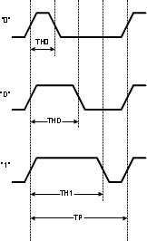 Figure 1. Single-Wire Interface (SWIF) Timing Diagram
6.7 Typical Characteristics
At TA = TJ = 25°C, Loop Voltage = 20V to 36V, unless otherwise specified.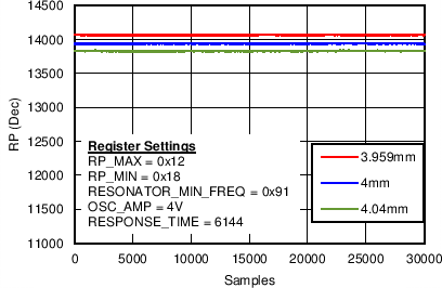
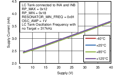
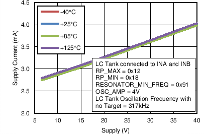
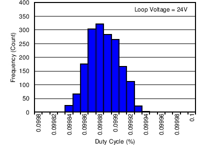 Figure 8. 0.1% Duty Cycle Distribution, PNP Mode
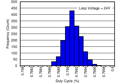 Figure 10. 0.8% Duty Cycle Distribution, PNP Mode
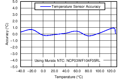
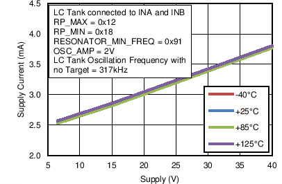
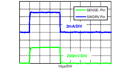
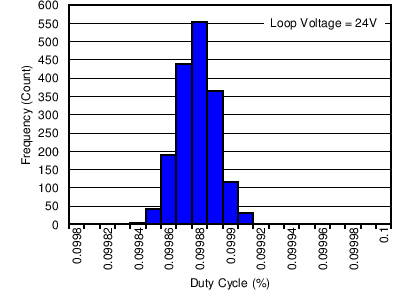 Figure 9. 0.1% Duty Cycle Distribution, NPN Mode
 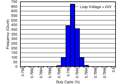 Figure 11. 0.8% Duty Cycle Distribution, NPN Mode
 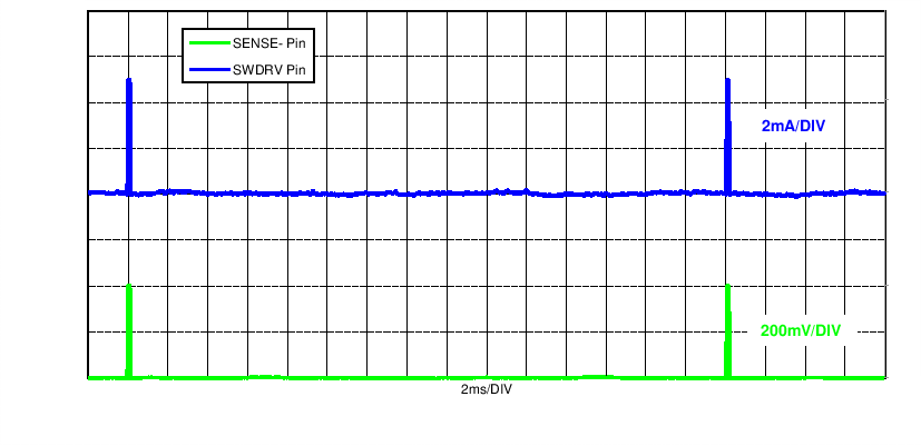 Figure 12. SWDRV and SENSE- Waveforms During Short Condition, SHORTCKT_DUTY_CYCLE = 0.1%
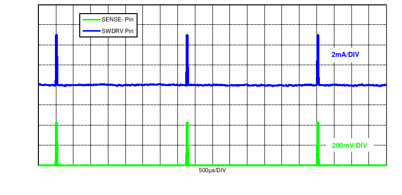 Figure 13. SWDRV and SENSE- Waveforms During Short Condition, SHORTCKT_DUTY_CYCLE = 0.8%