SNAS634B March 2014 – January 2016 LMP92066
PRODUCTION DATA.
- 1 Features
- 2 Applications
- 3 Description
- 4 Simplified Schematic
- 5 Revision History
- 6 Pin Configuration and Functions
- 7 Specifications
-
8 Detailed Description
- 8.1 Overview
- 8.2 Functional Block Diagram
- 8.3 Features Description
- 8.4 Device Functional Modes
- 8.5
Programming
- 8.5.1 Temperature Sensor Output Data Access Registers
- 8.5.2 DAC Input Data Registers
- 8.5.3 Temperature Sensor Status Register
- 8.5.4 Override Control Register
- 8.5.5 Override Data Registers
- 8.5.6 EEPROM Control Register
- 8.5.7 Software RESET Register
- 8.5.8 Access Control Register
- 8.5.9 Block I2C Access Control Register
- 8.5.10 I2C Address LOCK Register
- 8.5.11 Output Drive Supply Status Register
- 8.5.12 Device Version Register
- 8.5.13 EEPROM Burn Counter
- 8.5.14 LUT Coefficient Registers
- 8.5.15 LUT Control Registers
- 8.5.16 Notepad Registers
- 8.6 Register Map
- 9 Application and Implementation
- 10Power Supply Recommendations
- 11Layout
- 12Device and Documentation Support
- 13Mechanical, Packaging, and Orderable Information
Package Options
Mechanical Data (Package|Pins)
- PWP|16
Thermal pad, mechanical data (Package|Pins)
- PWP|16
Orderable Information
1 Features
- Internal 12-Bit Temperature Sensor
- Accuracy (–40°C to 120°C), ±3.2°C (maximum)
- Two Independent Transfer Functions Stored in EEPROM
- Dual-Analog Output
- Two 12-Bit DACs
- Output Range 0 V to 5 V or 0 V to –5 V
- High-Capacitive Load Tolerant, up to 10 µF
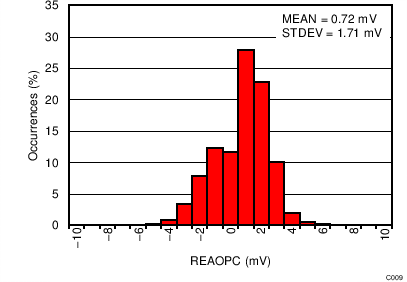
- Post-Calibration Accuracy ±2.4 mV (typical)
- Output On/Off Control Switching Time 50 ns (typical)
- Switching Time 50 ns (typical)
- RDSON 5 Ω (maximum)
- I2C Interface: Standard and Fast
- Nine Selectable Slave Addresses
- TIMEOUT Function
- VDD Supply Range 4.75 V to 5.25 V
- VIO Range 1.65 V to 3.6 V
- Specified Temperature Range –25°C to 120°C
- Operating Temperature Range –40°C to 125°C
2 Applications
- GaN or LDMOS PA Bias Controller
- Sensor Temperature Compensation
- Timing Circuit Temperature Compensation
3 Description
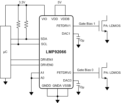
The LMP92066 is a highly integrated temperature-controlled dual DAC. Both DACs can be programmed by two independent, user-defined, temperature-to-voltage transfer functions stored in the internal EEPROM, allowing any temperature effects to be corrected without additional external circuitry. Once powered up, the device operates autonomously, without intervention from the system controller, to provide a complete solution for setting and compensating bias voltages and currents in control applications.
The LMP92066 has two analog outputs that support two output ranges: zero to plus five volts and zero to minus five volts. Each output can be switched to the load individually through the use of the dedicated control pin. The output switching is designed for rapid response, making the device suitable for the RF Power Amplifier biasing applications.
The EEPROM is verified for 100 write operations, enabling repeated field updates. The EEPROM programming is completed upon the user-issued I2C command.
The LMP92066’s digital ports interface to a variety of system controllers, as the dedicated VIO pin sets the digital I/O levels. The device is available in the thermally enhanced PowerPAD™ package, enabling precise PCB temperature measurement.
Device Information
| PART NUMBER | PACKAGE | BODY SIZE |
|---|---|---|
| LMP92066 | HTSSOP (16) | 5.00 mm x 4.40 mm |
4 Simplified Schematic

Residual Error After One Point Calibration
