SNVS737F October   2011  – June 2019 LMR24220

PRODUCTION DATA.  

  1. Features
  2. Applications
  3. Description
    1.     Device Images
      1.      Typical Application
  4. Revision History
  5. Pin Configuration and Functions
    1.     Pin Descriptions
  6. Specifications
    1. 6.1 Absolute Maximum Ratings
    2. 6.2 Recommended Operating Ratings
    3. 6.3 Electrical Characteristics
    4. 6.4 Typical Characteristics
  7. Detailed Description
    1. 7.1 Overview
    2. 7.2 Functional Block Diagram
    3. 7.3 Feature Description
      1. 7.3.1  CoT Control Circuit Overview
      2. 7.3.2  Start-up Regulator (VCC)
      3. 7.3.3  Regulation Comparator
      4. 7.3.4  Zero Coil Current Detect
      5. 7.3.5  Overvoltage Comparator
      6. 7.3.6  On-Time Timer, Shutdown
      7. 7.3.7  Current Limit
      8. 7.3.8  N-Channel MOSFET and Driver
      9. 7.3.9  Soft Start
      10. 7.3.10 Thermal Protection
  8. Application and Implementation
    1. 8.1 Application Information
    2. 8.2 Typical Application
      1. 8.2.1 Detailed Design Procedure
        1. 8.2.1.1 Custom Design With WEBENCH® Tools
        2. 8.2.1.2 External Components
      2. 8.2.2 Application Curve
  9. Layout
    1. 9.1 Layout Guidelines
    2. 9.2 Package Considerations
    3. 9.3 Thermal Derating
  10. 10Device and Documentation Support
    1. 10.1 Device Support
      1. 10.1.1 Development Support
        1. 10.1.1.1 Custom Design With WEBENCH® Tools
    2. 10.2 Receiving Notification of Documentation Updates
    3. 10.3 Community Resources
    4. 10.4 Trademarks
    5. 10.5 Electrostatic Discharge Caution
    6. 10.6 Glossary
  11. 11Mechanical, Packaging, and Orderable Information

Package Options

Mechanical Data (Package|Pins)
Thermal pad, mechanical data (Package|Pins)
Orderable Information

Typical Characteristics

Unless otherwise specified all curves are taken at VIN = 18 V with the configuration in the typical application circuit for
VOUT = 3.3 V (Figure 25) TA = 25°C.
LMR24220 30167604.png
Figure 1. VCC vs ICC
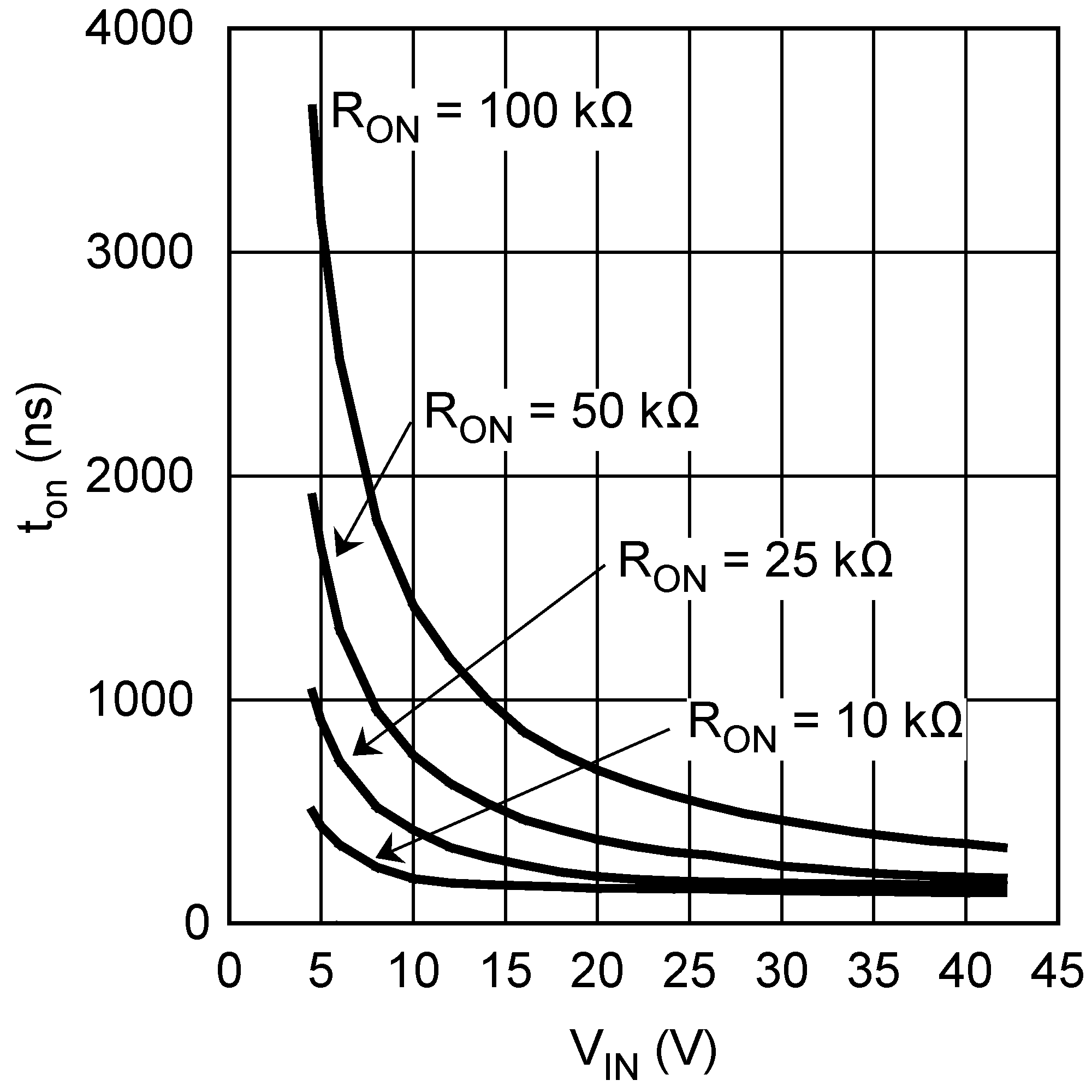
LMR24220 30167606.png
Figure 3. ton vs VIN
LMR24220 30167608.png
Figure 5. VFB vs Temperature
LMR24220 30167670.gif
VOUT = 3.3 V
Figure 7. Efficiency vs Load Current
LMR24220 30167672.gif
VOUT = 0.8 V
Figure 9. Efficiency vs Load Current
LMR24220 30167676.gif
VOUT = 3.3 V, 2 A Loaded
Figure 11. Power Up
LMR24220 30167615.gif
VOUT = 3.3 V, 2 A Loaded
Figure 13. Shutdown Transient
LMR24220 30167617.gif
VOUT = 3.3 V, 0.5 A Loaded
Figure 15. Discontinuous Mode Operation
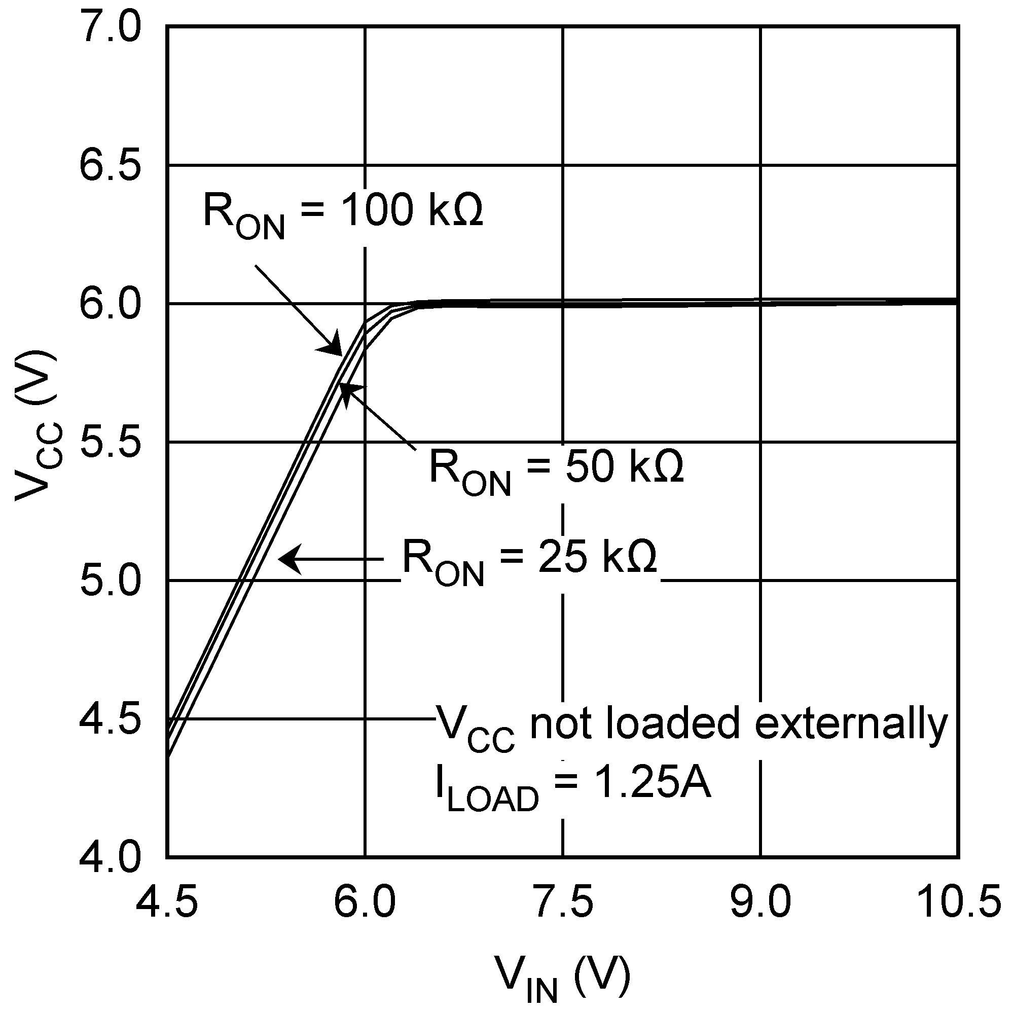
LMR24220 30167605.png
Figure 2. VCC vs VIN
LMR24220 30167675.gif
VOUT = 0.8 V
Figure 4. Switching Frequency, ƒSW vs VIN
LMR24220 30167609.png
Figure 6. RDS(on) vs Temperature
LMR24220 30167671.gif
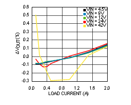
VOUT = 3.3 V
Figure 8. VOUT Regulation vs Load Current
LMR24220 30167673.gif
VOUT = 0.8 V
Figure 10. VOUT Regulation vs Load Current
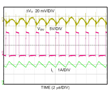
LMR24220 30167614.gif
VOUT = 3.3 V, 2 A Loaded
Figure 12. Start-up With Enable
LMR24220 30167616.gif
VOUT = 3.3 V, 2 A Loaded
Figure 14. Continuous Mode Operation
LMR24220 30167618.gif
VOUT = 3.3 V, 0.5 A to 2 A Loaded
Figure 16. DCM to CCM Transition