SNVSBV9 January   2021 LMR36015S

PRODUCTION DATA  

  1. Features
  2. Applications
  3. Description
  4. Revision History
  5. Description (continued)
  6. Device Comparison Table
  7. Pin Configuration and Functions
  8. Specifications
    1. 8.1 Absolute Maximum Ratings
    2. 8.2 ESD Ratings
    3. 8.3 Recommended Operating Conditions
    4. 8.4 Thermal Information
    5. 8.5 Electrical Characteristics
    6. 8.6 Timing Requirements
    7. 8.7 System Characteristics
    8. 8.8 Typical Characteristics
  9. Detailed Description
    1. 9.1 Overview
    2. 9.2 Functional Block Diagram
    3. 9.3 Feature Description
      1. 9.3.1 Power-Good Flag Output
      2. 9.3.2 Enable and Start-up
      3. 9.3.3 Current Limit and Short Circuit
      4. 9.3.4 Undervoltage Lockout and Thermal Shutdown
    4. 9.4 Device Functional Modes
      1. 9.4.1 Auto Mode
      2. 9.4.2 Forced PWM Operation
      3. 9.4.3 Dropout
      4. 9.4.4 Minimum Switch On-Time
  10. 10Application and Implementation
    1. 10.1 Application Information
    2. 10.2 Typical Application
      1. 10.2.1 Design 1: Low Power 24-V, 1.5-A PFM Converter
        1. 10.2.1.1 Design Requirements
        2. 10.2.1.2 Detailed Design Procedure
          1. 10.2.1.2.1  Custom Design With WEBENCH Tools
          2. 10.2.1.2.2  Choosing the Switching Frequency
          3. 10.2.1.2.3  Setting the Output Voltage
          4. 10.2.1.2.4  Inductor Selection
          5. 10.2.1.2.5  Output Capacitor Selection
          6. 10.2.1.2.6  Input Capacitor Selection
          7. 10.2.1.2.7  CBOOT
          8. 10.2.1.2.8  VCC
          9. 10.2.1.2.9  CFF Selection
            1. 10.2.1.2.9.1 External UVLO
          10. 10.2.1.2.10 Maximum Ambient Temperature
      2. 10.2.2 Application Curves
      3. 10.2.3 Design 2: High Density 24-V, 1.5-A FPWM Converter
        1. 10.2.3.1 Design Requirements
        2. 10.2.3.2 Detailed Design Procedure
        3. 10.2.3.3 Application Curves
    3. 10.3 What to Do and What Not to Do
  11. 11Power Supply Recommendations
  12. 12Layout
    1. 12.1 Layout Guidelines
      1. 12.1.1 Ground and Thermal Considerations
    2. 12.2 Layout Example
  13. 13Device and Documentation Support
    1. 13.1 Device Support
      1. 13.1.1 Development Support
        1. 13.1.1.1 Custom Design With WEBENCH® Tools
    2. 13.2 Documentation Support
      1. 13.2.1 Related Documentation
    3. 13.3 Receiving Notification of Documentation Updates
    4. 13.4 Support Resources
    5. 13.5 Trademarks
    6. 13.6 Electrostatic Discharge Caution
    7. 13.7 Glossary
  14. 14Mechanical, Packaging, and Orderable Information

Package Options

Mechanical Data (Package|Pins)
Thermal pad, mechanical data (Package|Pins)
Orderable Information

Application Curves

GUID-243BDD76-3257-4874-AEFE-C75642223A43-low.gif
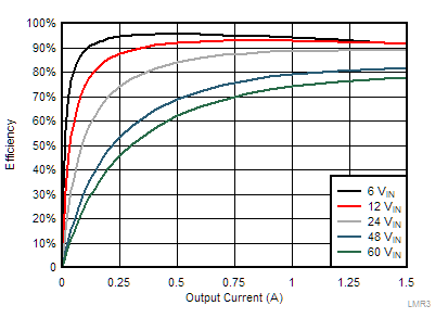
VOUT = 5 V 1000 kHz
Figure 10-28 Efficiency
GUID-49A65F34-C68D-48A2-9A88-BD651FD60173-low.gif
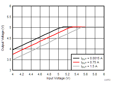
VOUT = 5 V 1000 kHz
Figure 10-30 Overall Dropout Characteristic
GUID-0346C968-4B19-47DB-94C7-4BDBC7EC4788-low.gif
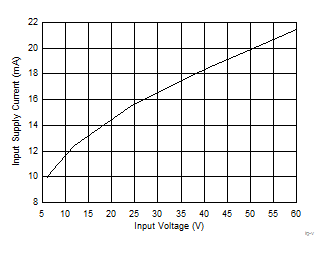
VOUT = 5 V IOUT= 0 A RFBT= 100 kΩ
Figure 10-32 Input Supply Current
GUID-1FE748CF-72E5-4E16-B8D6-AD9F450F42DA-low.jpg
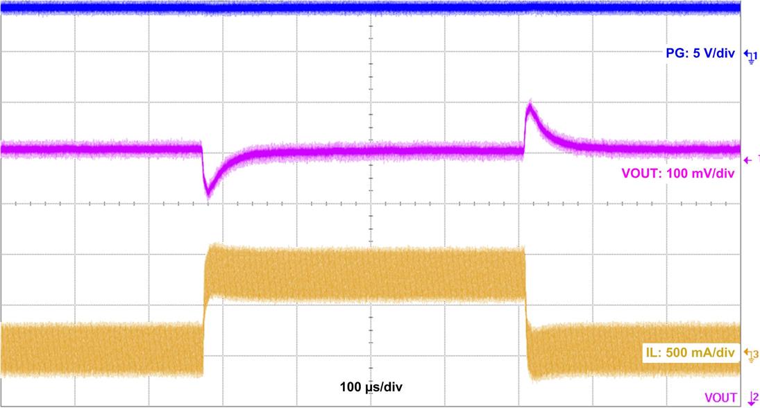
VOUT = 5 V 1000 kHz ILOAD= 0 A – 0.75 A
Slew Rate = 1 µs/A
Figure 10-34 Load Transient
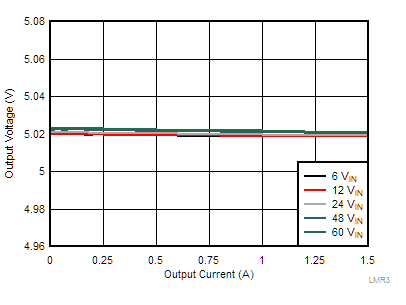
GUID-8C506B46-9982-442D-87FB-38E949D26775-low.gif
VOUT = 5 V 1000 kHz
Figure 10-29 Load Regulation
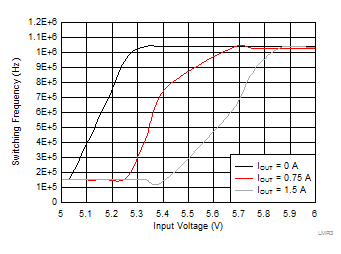
GUID-8387BD8C-25A1-4AB8-BA7C-F7B032084E62-low.gif
VOUT = 5 V 1000 kHz
Figure 10-31 Frequency Dropout Characteristic
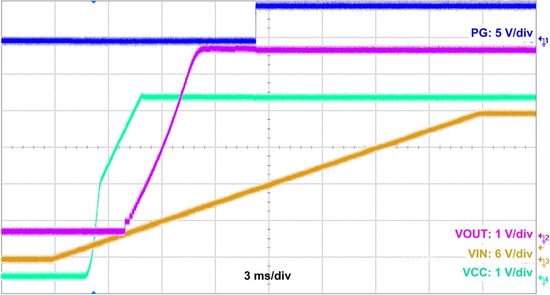
GUID-7B7D168D-9593-4A1D-9BE5-2D27C21CCBD0-low.jpg


VOUT = 5 V 1000 kHz
Figure 10-33 Start-Up Waveform
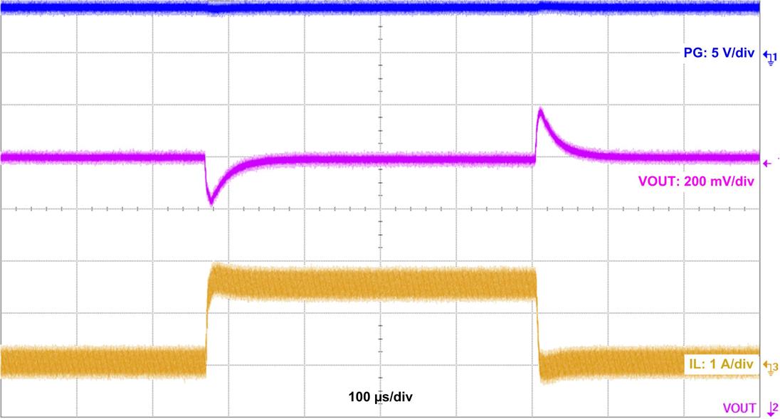
GUID-E70D7A5F-AACC-420B-85FE-81AAC8356B18-low.jpg
VOUT = 5 V Slew Rate = 1 µs/A 1000 kHz
ILOAD= 0 A – 1.5 A
Figure 10-35 Load Transient