-
LMR516x5 4.3V to 60V, 2.5A / 3.5A, Synchronous, Buck Converter With Low IQ
- 1
- 1 Features
- 2 Applications
- 3 Description
- 4 Device Comparison Table
- 5 Pin Configuration and Functions
- 6 Specifications
- 7 Detailed Description
- 8 Application and Implementation
- 9 Device and Documentation Support
- 10Revision History
- 11Mechanical, Packaging, and Orderable Information
- IMPORTANT NOTICE
Package Options
Mechanical Data (Package|Pins)
- DDC|6
Thermal pad, mechanical data (Package|Pins)
Orderable Information
LMR516x5 4.3V to 60V, 2.5A / 3.5A, Synchronous, Buck Converter With Low IQ
1 Features
- Functional Safety-Capable
- Configured for rugged industrial applications:
- 4.3V to 60V input voltage range
- 2.5A or 3.5A continuous output current
- Low operating quiescent current of 29μA
- 70ns minimum switching on time
- 400kHz amd 1.1MHz switching frequency
- Frequency spread spectrum (PFM variant)
- –40°C to 150°C junction temperature range
- 96% maximum duty cycle
- Monotonic start-up with prebiased output
- Short-circuit protection with hiccup mode
- Precision enable
- ±1% tolerance voltage reference
- Small design size and ease of use:
- Integrated synchronous rectification
- Internal compensation for ease of use
- SOT-23 package
- Various options in pin-to-pin compatible package
- PFM and forced PWM (FPWM) options
- Create a custom design using the LMR516x5 with the WEBENCH® Power Designer
3 Description
The LMR516x5 is a wide-VIN, easy-to-use, synchronous buck converter capable of driving up to 2.5A or 3.5A load current. With a wide input range of 4.3V to 60V, the device is designed for a wide range of industrial applications for power conditioning from an unregulated source.
The LMR516x5 operates at 400kHz or 1.1MHz switching frequency to support use of relatively small inductors for an optimized design size. The device has a pulse frequency modulation (PFM version) to realize high efficiency at light load and a forced pulse width modulation (PFM version) to achieve constant frequency and small output voltage ripple over the full load range, soft-start and compensation circuits are implemented internally, which allow the device to be used with minimal external components.
The device has built-in protection features, such as cycle-by-cycle current limit, hiccup mode short-circuit protection, and thermal shutdown in case of excessive power dissipation.
| PART NUMBER(3) | PACKAGE(1) | PACKAGE SIZE(2) |
|---|---|---|
| LMR51625 | DDC (SOT-23-THN, 6) | 2.9mm × 2.8mm |
| LMR51635 |
 Simplified Schematic
 Efficiency vs Output Current;
 VOUT = 5V, 400kHz
4 Device Comparison Table
| ORDERABLE PART NUMBER | OUTPUT CURRENT | FREQUENCY | PFM OR FPWM | SPREAD SPECTRUM | OUTPUT |
|---|---|---|---|---|---|
| LMR51625XDDCR | 2.5A | 400kHz | PFM | Yes | Adjustable |
| LMR51625XFDDCR | 2.5A | 400kHz | FPWM | No | Adjustable |
| LMR51625YDDCR | 2.5A | 1100kHz | PFM | Yes | Adjustable |
| LMR51625YFDDCR | 2.5A | 1100kHz | FPWM | No | Adjustable |
| LMR51635XDDCR | 3.5A | 400kHz | PFM | Yes | Adjustable |
| LMR51635XFDDCR | 3.5A | 400kHz | FPWM | No | Adjustable |
| LMR51635YDDCR | 3.5A | 1100kHz | PFM | Yes | Adjustable |
| LMR51635YFDDCR | 3.5A | 1100kHz | FPWM | No | Adjustable |
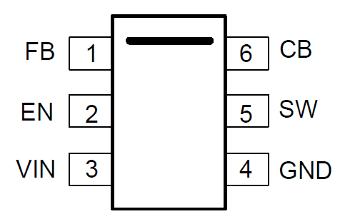
5 Pin Configuration and Functions
 Figure 5-1 6-Pin
SOT-23-THN,DDC Package(Top View)
Figure 5-1 6-Pin
SOT-23-THN,DDC Package(Top View)| PIN | TYPE(1) | DESCRIPTION | |
|---|---|---|---|
| NAME | NO | ||
| FB | 1 | A | Feedback input to the converter. Connect a resistor divider to set the output voltage. Never short this terminal to ground during operation. |
| EN | 2 | A | Precision enable input to the converter. Do not float. High = On, low = Off. Can be tied to VIN. Precision enable input allows an adjustable UVLO by an external resistor divider. |
| VIN | 3 | P | Supply input pin to the internal bias LDO and high-side FET. Connect to the input supply and input bypass capacitors CIN. Input bypass capacitors must be directly connected to this pin and GND. |
| GND | 4 | G | Power ground pins. Connected to the source of low-side FET internally. Connect to system ground, ground side of CIN and COUT. The path to CIN must be as short as possible. |
| SW | 5 | P | Switching output of the converter. Internally connected to source of the high-side FET and drain of the low-side FET. Connect to the power inductor. |
| CB | 6 | P | Bootstrap capacitor connection for high-side FET driver. Connect a high quality 100nF capacitor from this pin to the SW pin. |
6 Specifications
6.1 Absolute Maximum Ratings
| MIN | MAX | UNIT | ||
|---|---|---|---|---|
| Input voltage | VIN to GND | –0.3 | 63 | V |
| Input voltage | EN to GND | –0.3 | VIN + 0.3 | V |
| Input voltage | FB to GND | –0.3 | 5.5 | V |
| Output voltage | SW to GND | –0.3 | 63 | V |
| Output voltage | SW to GND less than 10ns transients | –3.5 | 65 | V |
| Output voltage | CB to SW | –0.3 | 5.5 | V |
| Junction temperature TJ | –40 | 150 | °C | |
| Storage temperature, Tstg | –55 | 150 | °C | |
functional operation of the device at these or any other conditions beyond those listed under Recommended Operating Conditions.
If used outside the Recommended Operating Conditions but within the Absolute Maximum Ratings, the device may not be fully
functional, and this may affect device reliability, functionality, performance, and shorten the device lifetime.