SLCS136U August 1999 – October 2020 LMV331 , LMV339 , LMV393
PRODUCTION DATA
- 1 Features
- 2 Applications
- 3 Description
- 4 Revision History
- 5 Pin Configuration and Functions
-
6 Specifications
- 6.1 Absolute Maximum Ratings
- 6.2 ESD Ratings
- 6.3 Recommended Operating Conditions
- 6.4 Thermal Information
- 6.5 Electrical Characteristics, VCC+ = 2.7 V
- 6.6 Electrical Characteristics, VCC+ = 5 V
- 6.7 Switching Characteristics, VCC+ = 2.7 V
- 6.8 Switching Characteristics, VCC+ = 5 V
- 6.9 Typical Characteristics
- 7 Detailed Description
- 8 Application and Implementation
- 9 Power Supply Recommendations
- 10Layout
- 11Device and Documentation Support
- 12Mechanical, Packaging, and Orderable Information
Package Options
Refer to the PDF data sheet for device specific package drawings
Mechanical Data (Package|Pins)
- DBV|5
- DCK|5
Thermal pad, mechanical data (Package|Pins)
Orderable Information
6.9 Typical Characteristics
Unless otherwise specified, VS = +5V, single supply, TA = 25°C
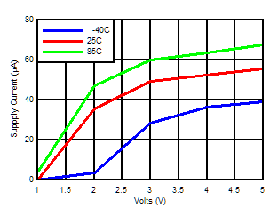 Figure 6-1 Supply Current vs Supply Voltage Output High (LMV33x)
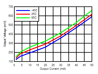 Figure 6-3 Output Voltage vs Output Current
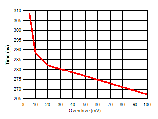 Figure 6-5 Response Time vs Input Overdrives Negative Transition (VCC=5 V)
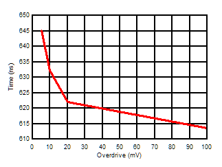 Figure 6-7 Response Time vs Input Overdrives Negative Transition (VCC = 2.7 V)
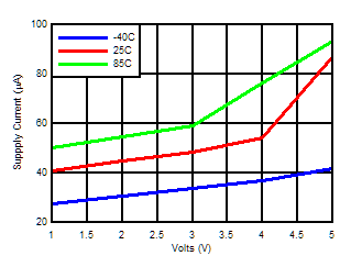 Figure 6-2 Supply Current vs Supply Voltage Output Low (LMV33x)
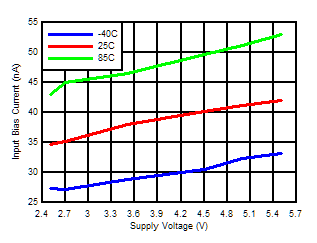 Figure 6-4 Input Bias Current vs Supply Voltage
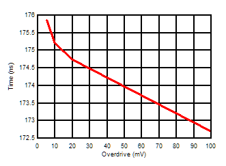 Figure 6-6 Response Time vs Input Overdrives Positive Transition (VCC = 5 V)
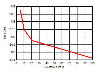 Figure 6-8 Response Time vs Input Overdrives Positive Transition (VCC = 2.7 V)