The LMV60x devices are single, dual, and quad low-voltage, low-power operational amplifiers. They are designed specifically for low-voltage, general-purpose applications. Other important product characteristics are low input bias current, rail-to-rail output, and wide temperature range. The LMV60x have 29-nV voltage noise at 10 KHz, 1-MHz GBW, 1-V/µs slew rate, 0.25-mV Vos. The LMV60x operates from a single supply voltage as low as 2.7 V, while drawing 100-µA (typical) quiescent current. In shutdown mode, the current can be reduced to 45 pA.
The industrial-plus temperature range of −40°C to 125°C allows the LMV60x to accommodate a broad range of extended environment applications.
The LMV601 offers a shutdown pin that can be used to disable the device. Once in shutdown mode, the supply current is reduced to 45 pA (typical).
The LMV601 is offered in the tiny 6-pin SC70 package, the LMV602 in space-saving 8-pin VSSOP and SOIC, and the LMV604 in 14-pin TSSOP and SOIC. These small package amplifiers offer an ideal solution for applications requiring minimum PCB footprint. Applications with area constrained printed-circuit board requirements include portable and battery-operated electronics.
PART NUMBER | PACKAGE | BODY SIZE (NOM) |
---|---|---|
LMV601 | SC70 (6) | 2.00 mm × 1.25 mm |
LMV602 | SOIC (8) | 4.90 mm × 3.91 mm |
VSSOP (8) | 3.00 mm × 3.00 mm | |
LMV604 | SOIC (8) | 4.90 mm × 3.91 mm |
TSSOP (14) | 5.00 mm × 4.40 mm |
Changes from B Revision (March 2013) to C Revision
Changes from A Revision (March 2012) to B Revision
PIN | I/O | DESCRIPTION | |
---|---|---|---|
NAME | NO. | ||
GND | 2 | P | Supply negative input |
+IN | 1 | I | Noninverting input |
–IN | 3 | I | Inverting input |
OUT | 4 | O | Output |
SHDN | 5 | I | Active low enable input |
V+ | 6 | P | Positive supply input |
PIN | I/O | DESCRIPTION | ||
---|---|---|---|---|
NAME | NO. | |||
LMV602 | LMV604 | |||
+INA | 3 | 3 | I | Noninverting input, channel A |
+INB | 5 | 5 | I | Noninverting input, channel B |
+INC | — | 10 | I | Noninverting input, channel C |
+IND | — | 12 | I | Noninverting input, channel D |
–INA | 2 | 2 | I | Inverting input, channel A |
–INB | 6 | 6 | I | Inverting input, channel B |
–INC | — | 9 | I | Inverting input, channel C |
–IND | — | 13 | I | Inverting input, channel D |
OUTA | 1 | 1 | O | Output, channel A |
OUTB | 7 | 7 | O | Output, channel B |
OUTC | — | 8 | O | Output, channel C |
OUTD | — | 14 | O | Output, channel D |
V+ | 8 | 4 | P | Positive (highest) power supply |
V– | 4 | 11 | P | Negative (lowest) power supply |
MIN | MAX | UNIT | |||
---|---|---|---|---|---|
Differential input voltage | ±Supply Voltage | ||||
Supply voltage, (V+) – (V–) | 6 | V | |||
Output short circuit to V+ | See(3) | ||||
Output short circuit to V– | See(4) | ||||
Junction temperature, TJ(5) | 150 | °C | |||
Storage temperature, Tstg | –65 | 150 | °C |
VALUE | UNIT | |||
---|---|---|---|---|
V(ESD) | Electrostatic discharge | Human-body model (HBM)(1)(1) | ±2000 | V |
Machine model (MM)(2) | ±200 |
MIN | MAX | UNIT | ||
---|---|---|---|---|
Supply voltage | 2.7 | 5.5 | V | |
Temperature | –40 | 125 | °C |
THERMAL METRIC(1) | LMV601 | LMV602 | LMV604 | UNIT | |||
---|---|---|---|---|---|---|---|
DCK (SC70) |
D (SOIC) |
DGK (VSSOP) |
D (SOIC) |
PW (TSSOP) |
|||
6 PINS | 8 PINS | 8 PINS | 14 PINS | 14 PINS | |||
RθJA | Junction-to-ambient thermal resistance | 229.1 | 120.8 | 178.3 | 91.5 | 123.8 | °C/W |
RθJC(top) | Junction-to-case (top) thermal resistance | 116.1 | 65.2 | 68.4 | 49.7 | 50.5 | °C/W |
RθJB | Junction-to-board thermal resistance | 53.3 | 61.4 | 98.8 | 46 | 66.2 | °C/W |
ψJT | Junction-to-top characterization parameter | 8.8 | 16.1 | 9.8 | 12.4 | 6.3 | °C/W |
ψJB | Junction-to-board characterization parameter | 52.7 | 60.8 | 97.3 | 45.7 | 65.6 | °C/W |
PARAMETER | TEST CONDITIONS | MIN | TYP | MAX | UNIT | |
---|---|---|---|---|---|---|
SR | Slew rate | RL = 10 kΩ,(2) | 1 | V/µs | ||
GBW | Gain bandwidth product | RL = 100 kΩ, CL = 200 pF | 1 | MHz | ||
Φm | Phase margin | RL = 100 kΩ | 72 | deg | ||
Gm | Gain margin | RL = 100 kΩ | 20 | dB | ||
en | Input-referred voltage noise | f = 1 kHz | 40 | nV/√Hz | ||
in | Input-referred current noise | f = 1 kHz | 0.001 | pA/√Hz | ||
THD | Total harmonic distortion | f = 1 kHz, AV = 1 RL = 600 Ω, VIN = 1 VPP |
0.017% |
PARAMETER | TEST CONDITIONS | MIN | TYP | MAX | UNIT | ||
---|---|---|---|---|---|---|---|
VOS | Input offset voltage | LMV601 | 0.25 | 4 | mV | ||
LMV602 and LMV604 | 0.7 | 5 | |||||
TCVOS | Input offset voltage average drift | 1.9 | µV/°C | ||||
IB | Input bias current | 0.02 | pA | ||||
IOS | Input offset current | 6.6 | fA | ||||
IS | Supply current | Per amplifier | 107 | 200 | µA | ||
Shutdown mode, VSD = 0 V (LMV601) | 0.033 | 1 | µA | ||||
CMRR | Common-mode rejection ratio | 0 V ≤ VCM ≤ 4 V | 86 | dB | |||
PSRR | Power supply rejection ratio | 2.7 V ≤ V+ ≤ 5 V | 82 | dB | |||
VCM | Input common-mode voltage | For CMRR ≥ 50 dB | 0 | 4 | V | ||
AV | Large signal voltage gain(2) | RL = 10 kΩ to 2.5 V | 116 | dB | |||
VO | Output swing | RL = 10 kΩ to 2.5 V | Swing high | 7 | 30 | mV | |
Swing low | 30 | 7 | |||||
IO | Output short-circuit current | Sourcing | 113 | mA | |||
Sinking | 75 | ||||||
ton | Turnon time from shutdown | (LMV601) | 5 | µs | |||
VSD | Shutdown pin voltage range | ON mode (LMV601) | 3.1 | 5 | V | ||
Shutdown mode (LMV601) | 0 | 0.8 |
PARAMETER | TEST CONDITIONS | MIN | TYP | MAX | UNIT | |
---|---|---|---|---|---|---|
SR | Slew rate | RL = 10 kΩ,(1) | 1 | V/µs | ||
GBW | Gain bandwidth product | RL = 100 kΩ, CL = 200 pF | 1 | MHz | ||
Φm | Phase margin | RL = 100 kΩ | 72 | ° | ||
Gm | Gain margin | RL = 100 kΩ | 20 | dB | ||
en | Input-referred voltage noise | f = 1 kHz | 39 | nV/√Hz | ||
in | Input-referred current noise | f = 1 kHz | 0.001 | pA/√Hz | ||
THD | Total harmonic distortion | f = 1 kHz, AV = 1 RL = 600 Ω, VIN = 1 VPP |
0.012% |
The LMV60x family of amplifiers features low-voltage, low-power, and rail-to-rail output operational amplifiers designed for low-voltage portable applications. The family is designed using all CMOS technology. This results in an ultra-low input bias current. The LMV601 has a shutdown option, which can be used in portable devices to increase battery life.
A simplified schematic of the LMV60x family of amplifiers is shown in Functional Block Diagram. The PMOS input differential pair allows the input to include ground. The output of this differential pair is connected to the Class AB turnaround stage. This Class AB turnaround has a lower quiescent current, compared to regular turnaround stages. This results in lower offset, noise, and power dissipation, while slew rate equals that of a conventional turnaround stage. The output of the Class AB turnaround stage provides gate voltage to the complementary common-source transistors at the output stage. These transistors enable the device to have rail-to-rail output.
This patented folded cascode stage has a combined class AB amplifier stage, which replaces the conventional folded cascode stage. Therefore, the class AB folded cascode stage runs at a much lower quiescent current compared to conventional folded cascode stages. This results in significantly smaller offset and noise contributions. The reduced offset and noise contributions in turn reduce the offset voltage level and the voltage noise level at the input of the LMV60x. Also the lower quiescent current results in a high open-loop gain for the amplifier. The lower quiescent current does not affect the slew rate of the amplifier nor its ability to handle the total current swing coming from the input stage.
The input voltage noise of the device at low frequencies, below 1 kHz, is slightly higher than devices with a BJT input stage. However, the PMOS input stage results in a much lower input bias current and the input voltage noise drops at frequencies above 1 kHz.
The LMV60x amplifiers have a PMOS input stage. As a result, they have a much lower input bias current than devices with BJT input stages. This feature makes these devices ideal for sensor circuits. A typical curve of the input bias current of the LMV601 is shown in Figure 41.
The LMV601 is capable of being turned off to conserve power and increase battery life in portable devices. Once in shutdown mode the supply current is drastically reduced, 1 µA maximum, and the output is tri-stated.
The device is disabled when the shutdown pin voltage is pulled low. The shutdown pin must never be left unconnected. Leaving the pin floating results in an undefined operation mode and the device may oscillate between shutdown and active modes.
The LMV601 typically turns on 2.8 µs after the shutdown voltage is pulled high. The device turns off in less than 400 ns after shutdown voltage is pulled low. Figure 42 and Figure 43 show the turnon and turnoff time of the LMV601, respectively. To reduce the effect of the capacitance added to the circuit by the scope probe, in the turnoff time circuit a resistive load of 600 Ω is added. Figure 44 and Figure 45 show the test circuits used to obtain the two plots.
NOTE
Information in the following applications sections is not part of the TI component specification, and TI does not warrant its accuracy or completeness. TI’s customers are responsible for determining suitability of components for their purposes. Customers should validate and test their design implementation to confirm system functionality.
The LMV60x family of amplifiers features low-voltage, low-power, and rail-to-rail output operational amplifiers designed for low-voltage portable applications.
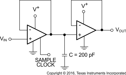
The lower input bias current of the LMV601 results in a very high input impedance. The output impedance when the device is in shutdown mode is quite high. These high impedances, and the ability of the shutdown pin to be derived from a separate power source, make LMV601 a good choice for sample and hold circuits. The sample clock must be connected to the shutdown pin of the amplifier to rapidly turn the device on or off.
Figure 46 shows the schematic of a simple sample-and-hold circuit. When the sample clock is high, the first amplifier is in normal operation mode and the second amplifier acts as a buffer. The capacitor, which appears as a load on the first amplifier, is charging at this time. The voltage across the capacitor is that of the noninverting input of the first amplifier because it is connected as a voltage-follower. When the sample clock is low, the first amplifier is shut off, bringing the output impedance to a high value. The high impedance of this output, along with the very high impedance on the input of the second amplifier, prevents the capacitor from discharging. There is very little voltage droop while the first amplifier is in shutdown mode. The second amplifier, which is still in normal operation mode and is connected as a voltage-follower, also provides the voltage sampled on the capacitor at its output.
Do properly bypass the power supplies.
Do add series resistence to the output when driving capacitive loads, particularly cables, Muxes, and ADC inputs.
Do add series current-limiting resistors and external Schottky clamp diodes if input voltage is expected to exceed the supplies. Limit the current to 1 mA or less (1 kΩ per volt).
For proper operation, the power supplies must be properly decoupled. For decoupling the supply lines, TI recommends that 10-nF capacitors be placed as close as possible to the operational amplifier power supply pins. For a single supply, place a capacitor between V+ and V− supply leads. For dual supplies, place one capacitor between V+ and ground, and one capacitor between V– and ground.
To properly bypass the power supply, consider the placement of several components on the printed-circuit boad. A 6.8‑µF or greater tantalum capacitor must be placed at the point where the power supply for the amplifier is introduced onto the board. Another 0.1-µF ceramic capacitor must be placed as close as possible to the power supply pin of the amplifier. If the amplifier is operated in a single power supply, only the V+ pin must be bypassed with a 0.1-µF capacitor. If the amplifier is operated in a dual power supply, both V+ and V– pins must be bypassed.
It is good practice to use a ground plane on a printed-circuit board to provide all components with a low inductive ground connection.
TI recommends surface-mount components in 0805 size or smaller in the LMV601-N application circuits. Designers can take advantage of the VSSOP miniature sizes to condense board layout to save space and reduce stray capacitance.