SLVS582K April 2006 – December 2024 LP2950 , LP2951
PRODUCTION DATA
- 1
- 1 Features
- 2 Applications
- 3 Description
- 4 Pin Configuration and Functions
- 5 Specifications
- 6 Detailed Description
- 7 Application and Implementation
- 8 Device and Documentation Support
- 9 Revision History
- 10Mechanical, Packaging, and Orderable Information
Package Options
Mechanical Data (Package|Pins)
- LP|3
Thermal pad, mechanical data (Package|Pins)
Orderable Information
4 Pin Configuration and Functions
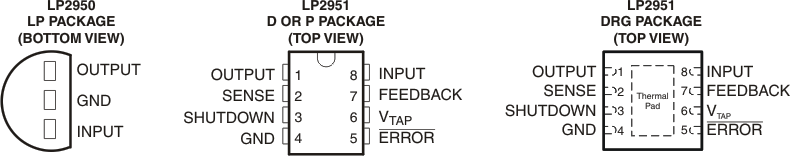
Table 4-1 Pin Functions
| PIN | TYPE(1) | DESCRIPTION | ||
|---|---|---|---|---|
| NAME | LP2950 | LP2951 | ||
| ERROR | — | 5 | O | Active-low open-drain error output. Goes low when VOUT drops by 6% of the nominal value. |
| FEEDBACK | — | 7 | I | Determines the output voltage. Connect to VTAP (with OUTPUT tied to SENSE) for fixed output option, or connect to a resistor divider for adjustable output option. |
| GND | 2 | 4 | — | Ground |
| INPUT | 3 | 8 | I | Input supply pin. Use a capacitor with a value of 1µF or larger from this pin to ground is recommended. See the Section 7.1.2 section for more information. |
| OUTPUT | 1 | 1 | O |
A capacitor is required from OUTPUT to GND for stability. For best transient response, use the nominal recommended value or larger ceramic capacitor from OUTPUT to GND (2). Place the output capacitor as close to output of the device as possible. See the Section 7.1.2 for more details. |
| SENSE | — | 2 | I | Senses the output voltage. Connect to OUTPUT (with FEEDBACK tied to VTAP) for fixed output option only. If using the device as adjustable output, this pin must be left floating. |
| SHUTDOWN | — | 3 | I | Active-high input. High signal disables the device; low signal enables the device. |
| VTAP | — | 6 | I | Connect to FEEDBACK for fixed output option. If using the device as adjustable output, this pin must be left floating. |
(1) I = Input; O = Output
(2) The nominal output capacitance
must be greater than 1μF. Throughout this document, the nominal derating on
these capacitors is 50%. Verify that the effective capacitance at the pin is
greater than 1μF.