SNVS095F May 2004 – March 2015 LP2952-N , LP2953
PRODUCTION DATA.
- 1 Features
- 2 Applications
- 3 Description
- 4 Revision History
- 5 Pin Configuration and Functions
- 6 Specifications
- 7 Detailed Description
-
8 Application and Implementation
- 8.1 Application Information
- 8.2
Typical Applications
- 8.2.1 Basic 5-V Regulator
- 8.2.2 5-V Current Limiter with Load Fault Indicator
- 8.2.3 Low Temperature Coefficient Current Sink
- 8.2.4 5-V Regulator With Error Flags for Low Battery and Out of Regulation
- 8.2.5 5-V Battery Powered Supply With Backup and Low Battery Flag
- 8.2.6 5-V Regulator With Timed Power-On Reset
- 8.2.7 5-V Regulator With Snap-ON and Snap-OFF Features and Hysteresis
- 8.2.8 5-V Regulator With Error Flags for Low Battery and Out of Regulation With Snap-ON or Snap-OFF Output
- 8.2.9 5-V Regulator With Timed Power-On Reset, Snap-ON and Snap-OFF Features, and Hysteresis
- 9 Power Supply Recommendations
- 10Layout
- 11Device and Documentation Support
- 12Mechanical, Packaging, and Orderable Information
Package Options
Mechanical Data (Package|Pins)
- D|16
Thermal pad, mechanical data (Package|Pins)
Orderable Information
10 Layout
10.1 Layout Guidelines
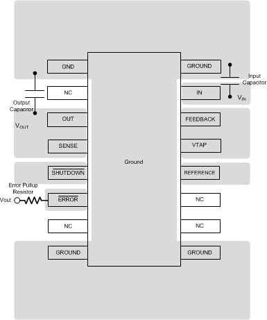
For best overall performance, place all circuit components on the same side of the circuit board and as near as practical to the respective LDO pin connections. Place ground return connections to the input and output capacitors, and to the LDO ground pin as close to each other as possible, connected by a wide, component-side, copper surface. The use of vias and long traces to create LDO circuit connections is strongly discouraged and negatively affects system performance. This grounding and layout scheme minimizes inductive parasitics, and thereby reduces load-current transients, minimizes noise, and increases circuit stability.
A ground reference plane is also recommended and is either embedded in the PCB itself or located on the bottom side of the PCB opposite the components. This reference plane serves to assure accuracy of the output voltage, shield noise, and behaves similar to a thermal plane to spread (or sink) heat from the LDO device. In most applications, this ground plane is necessary to meet thermal requirements.
10.2 Layout Example
 Figure 46. Layout Schematic
10.3 Power Dissipation: Heatsink Requirements (Industrial Temperature Range Devices)
The maximum allowable power dissipation for the LP2952 or LP2953 is limited by the maximum operating junction temperature (125°C) and the external factors that determine how quickly heat flows away from the part: the ambient temperature and the junction-to-ambient thermal resistance (RθJA) for the specific application.
The industrial temperature range (−40°C ≤ TJ ≤ 125°C) parts are manufactured in PDIP and surface-mount packages which contain a copper lead frame that allows heat to be effectively conducted away from the die, through the ground pins of the IC, and into the copper of the PC board. Details on heatsinking using PC board copper are covered later.
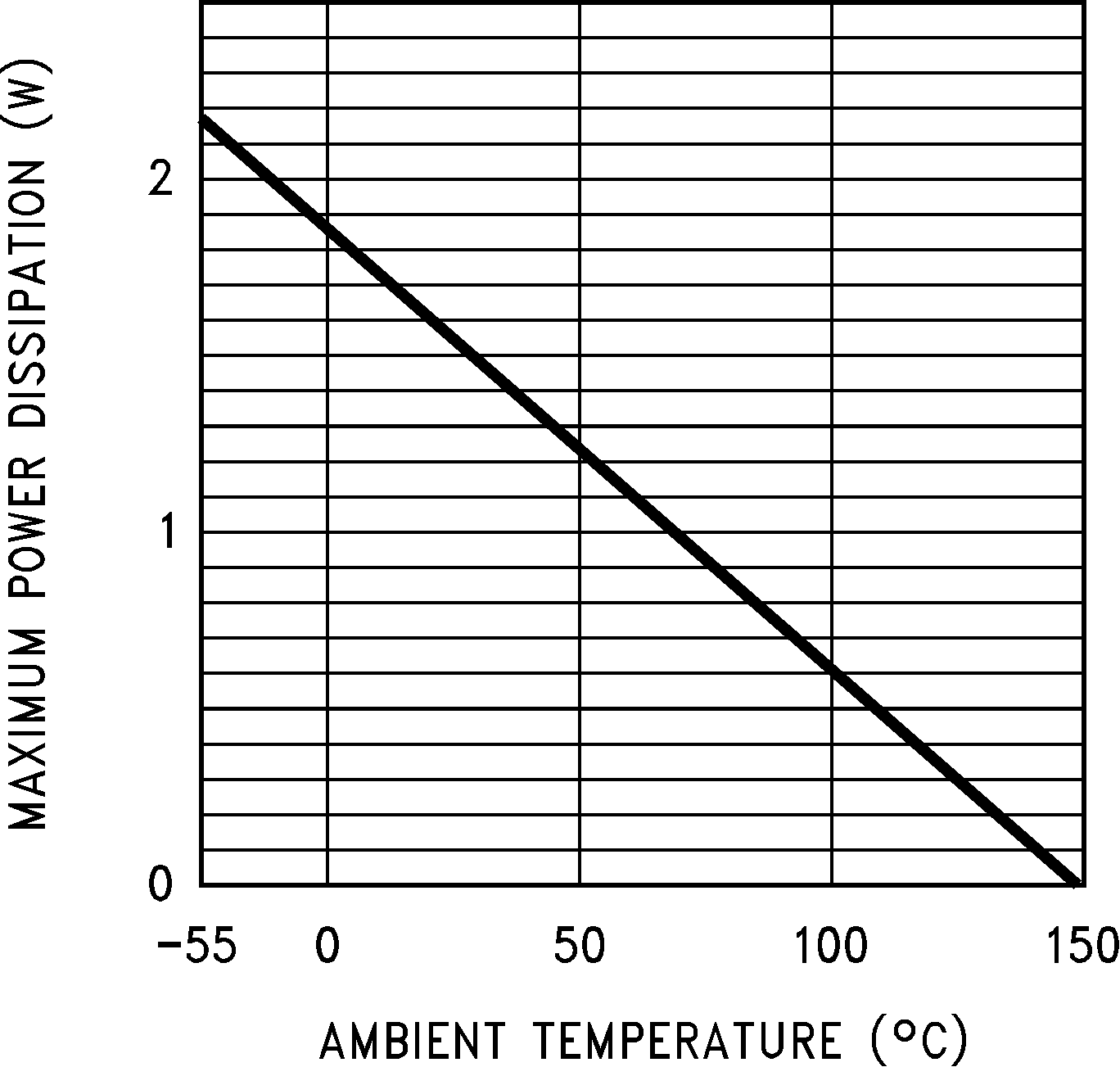
 Figure 47. Power Dissipation vs Ambient Temperature
for RθJA = 95°C/W
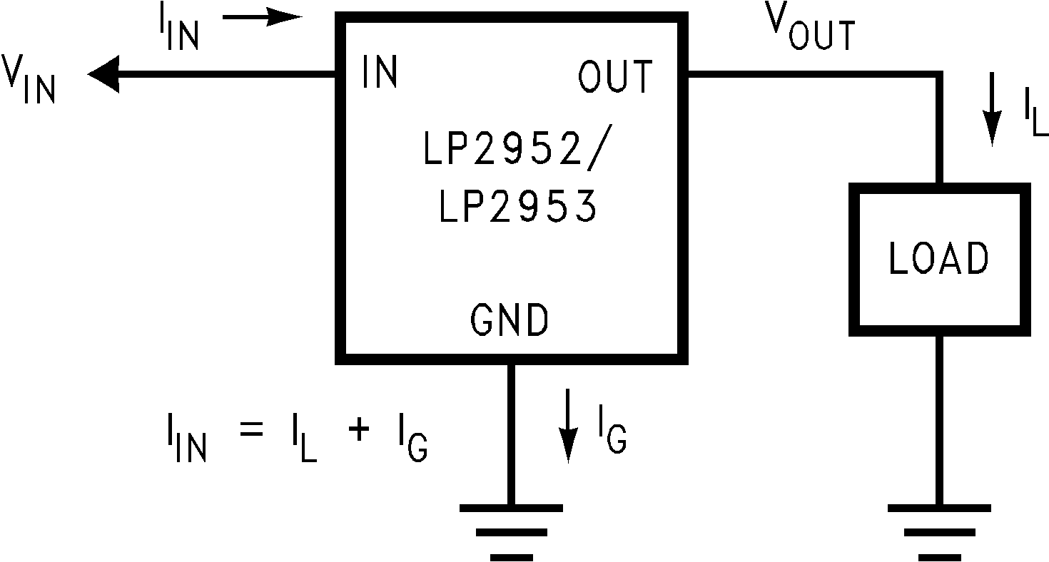
To determine if a heatsink is required, the maximum power dissipated by the regulator, P(MAX), must be calculated. It is important to remember that if the regulator is powered from a transformer connected to the AC line, the maximum specified AC input voltage must be used (because this produces the maximum DC input voltage to the regulator). Figure 48 shows the voltages and currents which are present in the circuit. The formula for calculating the power dissipated in the regulator is also shown in Figure 48:
 Figure 48. PTOTAL = (VIN − VOUT) IOUT + (VIN) IG
Current/Voltage Diagram
The next parameter which must be calculated is the maximum allowable temperature rise, TR(MAX). This is calculated by using the formula:
where
- TJ(MAX) is the maximum allowable junction temperature
- TA(MAX) is the maximum ambient temperature
Using the calculated values for TR(MAX) and P(MAX), the required value for junction-to-ambient thermal resistance, RθJA, can now be found.
The heatsink is made using the PC board copper. The heat is conducted from the die, through the lead frame (inside the part), and out the pins which are soldered to the PC board. The pins used for heat conduction are given in Table 2.
Table 2. Heat Conducting Pins
| PART | PACKAGE | PINS |
|---|---|---|
| LP2953IN, LP2953AIN | 16-pin PDIP | 4, 5, 12, 13 |
| LP2953IN-3.3, LP2953AIN-3.3 | ||
| LP2952IM, LP2952AIM | 16-pin surface mount (SOIC) | 1, 8, 9, 16 |
| LP2952IM-3.3, LP2952AIM-3.3 | ||
| LP2953IM, LP2953AIM | ||
| LP2953IM-3.3, LP2953AIM-3.3 |
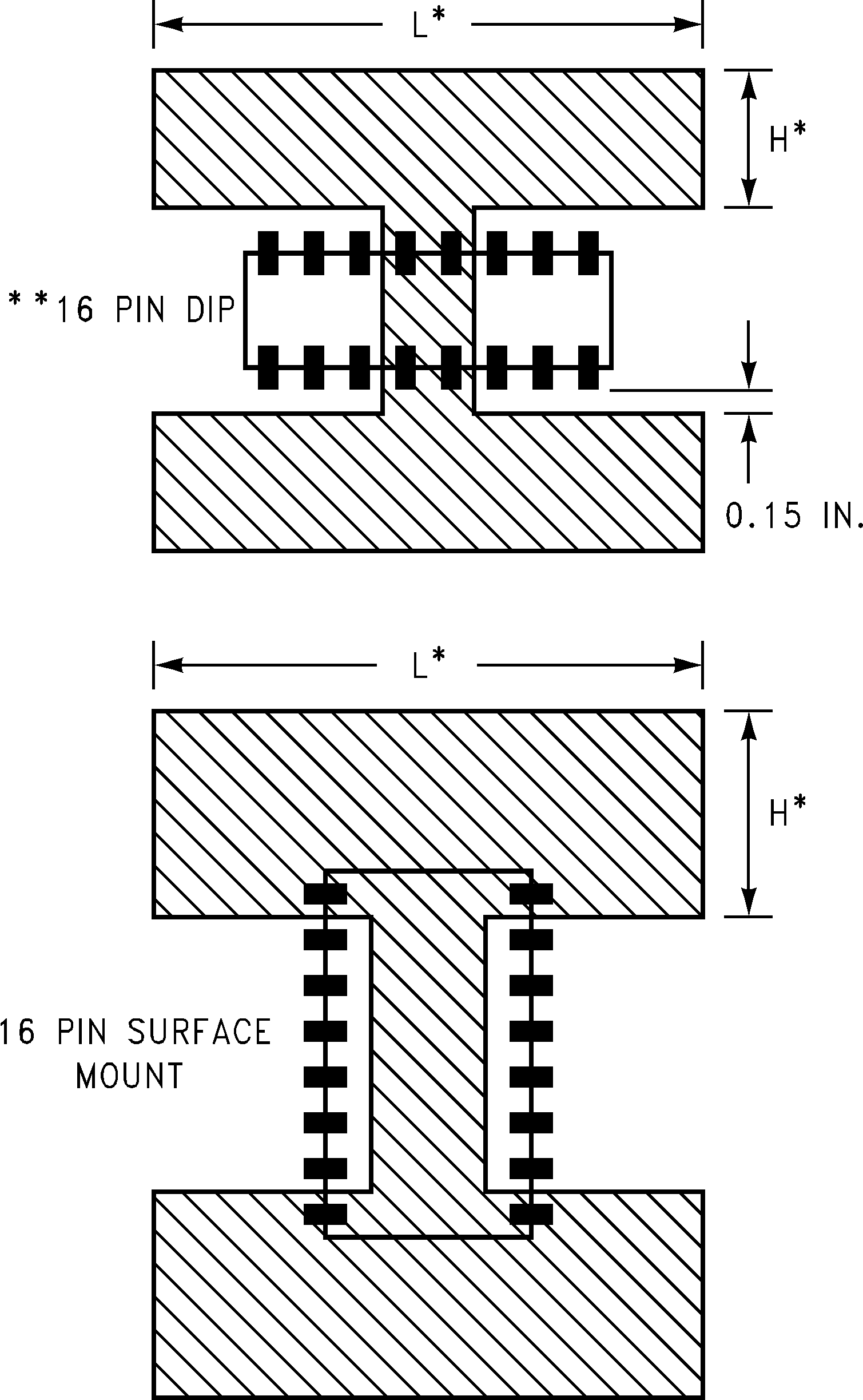
Figure 49 shows copper patterns which may be used to dissipate heat from the LP2952 and LP2953.

** 14-Pin PDIP is similar, see Table 2 for pins designated for heatsinking.