SNVS095F May 2004 – March 2015 LP2952-N , LP2953
PRODUCTION DATA.
- 1 Features
- 2 Applications
- 3 Description
- 4 Revision History
- 5 Pin Configuration and Functions
- 6 Specifications
- 7 Detailed Description
-
8 Application and Implementation
- 8.1 Application Information
- 8.2
Typical Applications
- 8.2.1 Basic 5-V Regulator
- 8.2.2 5-V Current Limiter with Load Fault Indicator
- 8.2.3 Low Temperature Coefficient Current Sink
- 8.2.4 5-V Regulator With Error Flags for Low Battery and Out of Regulation
- 8.2.5 5-V Battery Powered Supply With Backup and Low Battery Flag
- 8.2.6 5-V Regulator With Timed Power-On Reset
- 8.2.7 5-V Regulator With Snap-ON and Snap-OFF Features and Hysteresis
- 8.2.8 5-V Regulator With Error Flags for Low Battery and Out of Regulation With Snap-ON or Snap-OFF Output
- 8.2.9 5-V Regulator With Timed Power-On Reset, Snap-ON and Snap-OFF Features, and Hysteresis
- 9 Power Supply Recommendations
- 10Layout
- 11Device and Documentation Support
- 12Mechanical, Packaging, and Orderable Information
Package Options
Mechanical Data (Package|Pins)
- D|16
Thermal pad, mechanical data (Package|Pins)
Orderable Information
7 Detailed Description
7.1 Overview
The LP2952 and LP2953 are very high accuracy micropower voltage regulators with low quiescent current (130 μA, typical) and low dropout voltage (typically 60 mV at light loads and 490 mV at 250 mA). They are ideally suited for use in battery-powered systems.
The LP2952 and LP2953 block diagram contains several features, including:
- Very high accuracy 1.23-V reference.
- Internal protection circuitry, such as thermal foldback current limit, thermal shutdown protection, and reverse battery-input protection.
- Fixed 5-V and 3.3-V versions.
- Error flag output which may be used for a power-on reset.
- Shutdown input, allowing turn off the regulator when the SHUTDOWN pin is pulled low.
LP2953 versions only:
7.2 Functional Block Diagrams
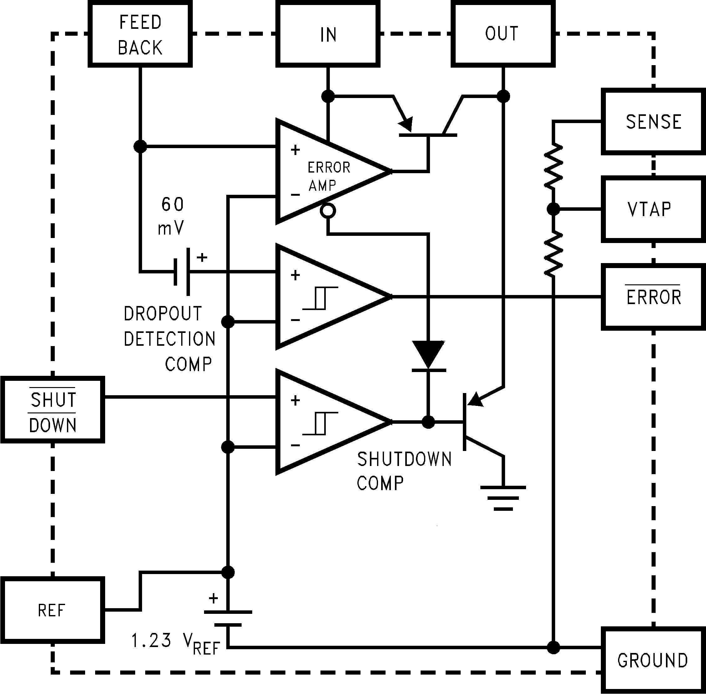
 Figure 28. LP2952 Block Diagram
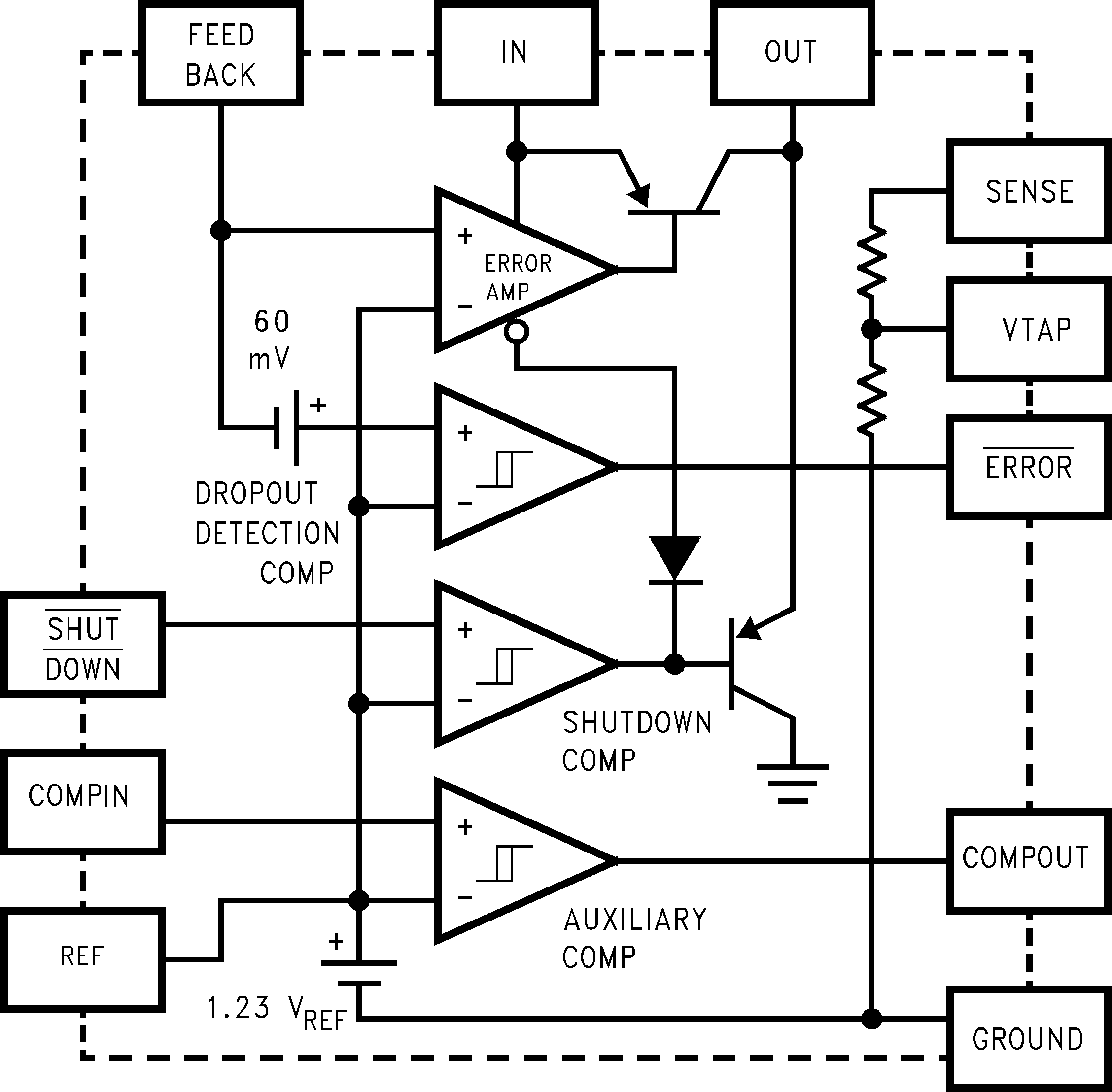
 Figure 29. LP2953 Block Diagram
7.3 Feature Description
7.3.1 Fixed Voltage Options and Programmable Voltage Version
The LP2952 and LP2953 provide 2 fixed output options: 3.3 V and 5 V. To meet different requirements for the application, they can also be used as programmable voltage regulators with external resistor networks; see Application Information for more details.
7.3.2 High-Accuracy Output Voltage
With special and careful design to minimize all contributions to the output voltage error, the LP2952 and LP2953 distinguished themselves as very high output voltage accuracy micropower LDO. This includes a tight initial tolerance (0.5% typical), extremely good load and line regulation, and a very low output voltage temperature coefficient, making the part an ideal a low-power voltage reference.
7.3.3 Error Detection Comparator Output
The LP2952 and LP2953 will generate a logic low output when the output falls out of regulation by more than approximately 5%. See Application Information for more details.
7.3.4 Auxiliary Comparator
An auxiliary comparator is designed for customer special purpose when shutdown is activated. This block is still active and can be used to generate fault detection, low input line detection signal for system controllers. The comparator output level is CMOS- or TTL-compatible. See Application Information for more details.
7.3.5 Short-Circuit Protection (Current Limit)
The internal current limit circuit is used to protect the LDO against high-load current faults or shorting events. The LDO is not designed to operate in a steady-state current limit. During a current-limit event, the LDO sources constant current. Therefore, the output voltage falls when load impedance decreases. Note also that if a current limit occurs and the resulting output voltage is low, excessive power may be dissipated across the LDO resulting in a thermal shutdown of the output. A thermal foldback feature limits the short-circuit current to protect the regulator from damage under all load conditions. If the OUT pin is forced below 0 V before SHUTDOWN goes high and the load current required exceeds the thermal foldback current limit, the device may not start up correctly.
7.3.6 Thermal Protection
The device contains a thermal shutdown protection circuit to turn off the output current when excessive heat is dissipated in the LDO. The thermal time-constant of the semiconductor die is fairly short, and thus the output cycles on and off at a high rate when thermal shutdown is reached until the power dissipation is reduced. The internal protection circuitry of the device is designed to protect against thermal overload conditions. The circuitry is not intended to replace a proper heatsink. Continuously running the device into thermal shutdown degrades its reliability.
7.4 Device Functional Mode
7.4.1 Shutdown Mode
When pulling the SHUTDOWN pin to low level, the LP2952 and LP2953 will enter shutdown mode, and a very low quiescent current is consumed. This function is designed for applications which needs a shutdown mode to effectively enhance battery life cycle. When the SHUTDOWN pin is low the automatic output discharge circuity will be active. See Application Information for more details.
Operation with 30 V ≥ VIN > VOUT(TARGET) + 1 V
The device operate if the input voltage is equal to, or exceeds, VOUT(TARGET) + 1 V, and SHUTDOWN is pulled to high level. At input voltages below the minimum VIN requirement, the devices do not operate correctly and output voltage may not reach target value.