SNVS481M November 2006 – December 2015 LP3910
PRODUCTION DATA.
- 1 Features
- 2 Applications
- 3 Description
- 4 Revision History
- 5 Device Comparison Tables
- 6 Pin Configuration and Functions
-
7 Specifications
- 7.1 Absolute Maximum Ratings
- 7.2 ESD Ratings
- 7.3 Recommended Operating Conditions
- 7.4 Thermal Information
- 7.5 Electrical Characteristics
- 7.6 Electrical Characteristics: I2C Interface
- 7.7 Electrical Characteristics: Li-Ion Battery Charger
- 7.8 Detection and Timing
- 7.9 Output Electrical Characteristics: CHG, STAT
- 7.10 Output Electrical Characteristics: NRST, IRQB, ONSTAT
- 7.11 Input Electrical Characteristics: USBSUSP, USBISEL
- 7.12 Input Electrical Characteristics: POWERACK, ONOFF, LDO2EN, BUCK1EN
- 7.13 Electrical Characteristics: LDO1 Low Dropout Linear Regulators
- 7.14 Electrical Characteristics: LDO2 Low Dropout Linear Regulator
- 7.15 Electrical Characteristics: Buck1 Converter
- 7.16 Electrical Characteristics: Buck2 Converter
- 7.17 Electrical Characteristics: Buck-Boost
- 7.18 Electrical Characteristics: ADC
- 7.19 I2C Timing Requirements
- 7.20 USB Timing Requirements
- 7.21 Typical Characteristics
-
8 Detailed Description
- 8.1 Overview
- 8.2 Functional Block Diagram
- 8.3
Feature Description
- 8.3.1 Buck1, Buck2: Synchronous Step-Down Magnetic DC-DC Converters
- 8.3.2 Buck-Boost: Synchronous Buck-Boost Magnetic DC-DC Converter
- 8.3.3 Linear Low Dropout Regulators (LDOs)
- 8.3.4 Li-Ion Linear Charger
- 8.3.5 ADC
- 8.3.6 Interrupt Request Output
- 8.3.7 Power-On-Reset
- 8.3.8 Thermal Shutdown and Thermal Alarm
- 8.3.9 NRST Pin
- 8.3.10 Operation Without I2C Interface
- 8.3.11 I2C Master Power Concern
- 8.3.12 System Operation When the Load Current Exceeds the USB or Adapter Current Limit
- 8.3.13 Power Routing
- 8.3.14 Battery Monitor
- 8.3.15 External Power and Battery Detection
- 8.3.16 USB Suspend Mode
- 8.3.17 Setting the USB Current Limit
- 8.3.18 Control Registers
- 8.4 Device Functional Modes
- 8.5 Programming
- 8.6
Register Maps
- 8.6.1 LDO1 Control Register
- 8.6.2 BATTLOW Register (04)H Battery Low Alarm Register
- 8.6.3 PON Register (00)H Power-On Event Register
- 8.6.4 CHCTL Register (01)H Charger Control Register
- 8.6.5 CHSPV Register (02)H Charger Supervisor Register
- 8.6.6 ILIMIT Register (03)H Current Limit Register
- 8.6.7 ADCC Register (0a)H ADC Control Register
- 8.6.8 ADCD Register (0b)H ADC Output Data Register
- 8.6.9 IMR Register (0c)H Interrupt Mask Register
- 8.6.10 IRQ Register (0d)H Interrupt Request Register
- 8.6.11 LDO1 Control Register (08)H
- 8.6.12 LDO2 Control Register
- 8.6.13 Buck1, Buck2 Control Registers and BUCK1EN Pin
- 8.6.14 Buck-Boost Control Register
-
9 Application and Implementation
- 9.1 Application Information
- 9.2
Typical Application
- 9.2.1 Design Requirements
- 9.2.2 Detailed Design Procedure
- 9.2.3 Application Curves
- 10Power Supply Recommendations
- 11Layout
- 12Device and Documentation Support
- 13Mechanical, Packaging, and Orderable Information
Package Options
Mechanical Data (Package|Pins)
- NJV|48
Thermal pad, mechanical data (Package|Pins)
Orderable Information
7 Specifications
7.1 Absolute Maximum Ratings
over operating free-air temperature range (unless otherwise noted)(1)(2)(3)| MIN | MAX | UNIT | ||
|---|---|---|---|---|
| Supply voltage | CHG_DET | –0.3 | 6.5 | V |
| Battery voltage | VBATT1, 2, 3 | –0.3 | 5 | V |
| Voltage | USBPWR, VIN1,VIN2,VIN3,VIN4, VDD1,VDD2,VDD3 | –0.3 | 6.2 | V |
| All other pins | –0.3 | VDD + 0.3 | V | |
| Power dissipation (TA = 70°C)(4) | 2.6 | W | ||
| Storage temperature, Tstg | –45 | 150 | ºC | |
(1) Stresses beyond those listed under Absolute Maximum Ratings may cause permanent damage to the device. These are stress ratings only, which do not imply functional operation of the device at these or any other conditions beyond those indicated under Recommended Operating Conditions. Exposure to absolute-maximum-rated conditions for extended periods may affect device reliability.
(2) All voltages are with respect to the potential at the GND pin.
(3) In applications where high power dissipation or poor package thermal resistance is present, the maximum ambient temperature may have to be derated. Maximum ambient temperature (TA-MAX) is dependent on the maximum operating junction temperature (TJ-MAX-OP = 125°C), the maximum power dissipation of the device in the application (PD-MAX), and the junction-to-ambient thermal resistance of the part/package in the application (RθJA), as given by the following equation: TA-MAX = TJ-MAX-OP − (RθJA × PD-MAX).
(4) Internal thermal shutdown circuitry protects the device from permanent damage. Thermal shutdown engages at TJ = 160°C (typical) and disengages at TJ = 140°C (typical).
7.2 ESD Ratings
| VALUE | UNIT | |||
|---|---|---|---|---|
| V(ESD) | Electrostatic discharge | Human-body model (HBM), per ANSI/ESDA/JEDEC JS-001(1) | ±2000 | V |
| Machine model | ±200 | |||
(1) JEDEC document JEP155 states that 500-V HBM allows safe manufacturing with a standard ESD control process.
7.3 Recommended Operating Conditions
over operating free-air temperature range (unless otherwise noted)(1)(2)(3)| MIN | NOM | MAX | UNIT | ||
|---|---|---|---|---|---|
| CHG_DET | 4.5 | 6 | V | ||
| USBPWR | 4.35 | 6 | V | ||
| VBATT1, 2, 3 | 0 | 4.5 | V | ||
| VIN1, VIN2, VIN3, VIN4, VDD1, VDD2, VDD3 | 2.5 | 6 | V | ||
| VDDIO | 2.5 | VDD | V | ||
| Junction temperature, TJ | –40 | 125 | °C | ||
| Ambient temperature, TA | –40 | 85 | °C | ||
| Power dissipation, TJ-MAX and TA-MAX | 1.6 | W | |||
(1) Junction-to-ambient thermal resistance is highly application and board-layout dependent. In applications where high maximum power dissipation exists, special care must be paid to thermal dissipation issues in board design.
(2) Minimum and maximum limits are specified by design, test, or statistical analysis. Nominal numbers are not ensured, but do represent the most likely norm.
(3) Nominal values and limits are for TJ = 25°C.
7.4 Thermal Information
| THERMAL METRIC(1) | LP3910 | UNIT | |
|---|---|---|---|
| NJV (WQFN) | |||
| 48 PINS | |||
| RθJA | Junction-to-ambient thermal resistance | 25 | °C/W |
(1) For more information about traditional and new thermal metrics, see the Semiconductor and IC Package Thermal Metrics application report (SPRA953).
7.5 Electrical Characteristics
Unless otherwise noted, VDD = 5 V, VBATT = 3.6 V, and limits apply for TJ = 25°C.(1)(2)(3)(4)| PARAMETER | TEST CONDITIONS | MIN | TYP | MAX | UNIT | |
|---|---|---|---|---|---|---|
| IQ_BATT | Battery standby supply current | All circuits off except for POR and battery monitor. No adapter or USB power connected. | 6 | 20 | µA | |
| IQ_BATT | Battery standby supply current | All circuits off except for POR and battery monitor. No adapter or USB power connected. TJ = 0°C to 125°C |
20 | µA | ||
| VPOR | Power-on reset threshold | VDD falling edge | 1.9 | V | ||
| TSD | Thermal shutdown threshold | 160 | °C | |||
| TSDH | Thermal shutdown hysteresis | 20 | °C | |||
| TTH-ALERT | Thermal interrupt threshold | 115 | °C | |||
| VDDIO | IO supply | 2.5 | VDD | V | ||
| FCLK | Internal system clock frequency | 2 | MHz | |||
(1) All voltages are with respect to the potential at the GND pin.
(2) Minimum and maximum limits are specified by design, test, or statistical analysis. Typical numbers are not ensured, but do represent the most likely norm.
(3) Low ESR Surface-Mount Ceramic Capacitors (MLCCs) are used in setting electrical characteristics.
(4) This specification is ensured by design. Not tested during production.
7.6 Electrical Characteristics: I2C Interface
Unless otherwise noted, VDDIO = 3.6 V, and minimum and maximum limits apply for TJ = 0°C to 125°C.(1)(2)(3)(4)| PARAMETER | TEST CONDITIONS | MIN | TYP | MAX | UNIT | |
|---|---|---|---|---|---|---|
| VIL | Low level input voltage | I2C_SDA & I2C_SCL | 0.3 × VDDIO | V | ||
| VIH | High level input voltage | I2C_SDA & I2C_SCL | 0.7 × VDDIO | V | ||
| VOL | Low level output voltage | I2C_SDA & I2C_SCL | 0 | 0.2 × VDDIO | V | |
| VHYS | Schmitt trigger input hysterisis | I2C_SDA & I2C_SCL | 0.1 × VDDIO | V | ||
(1) All voltages are with respect to the potential at the GND pin.
(2) Minimum and maximum limits are specified by design, test, or statistical analysis.
(3) Low ESR Surface-Mount Ceramic Capacitors (MLCCs) are used in setting electrical characteristics.
(4) This specification is ensured by design.
7.7 Electrical Characteristics: Li-Ion Battery Charger
Unless otherwise noted, VDD = 5 V, VBATT = 3.6 V, CBATT = 4.7 µF, CCHG_DET = 10 µF, RIREF = 121 kΩ. Typical limits apply for TJ = 25°C; minimum and maximum limits apply for TJ = 0°C to 125°C, unless otherwise specified.(1)(2)(3)(4)| PARAMETER | TEST CONDITIONS | MIN | TYP | MAX | UNIT | |
|---|---|---|---|---|---|---|
| VUSB | Minimum external USB supply voltage | TJ = 25°C USB current limit = 500 mA |
4.15 | 4.25 | 4.35 | V |
| VUSB_HYST | USBPWR detect hysteresis | 110 | mV | |||
| CHG_DET | Minimum external adapter supply voltage range | TJ = 25°C Adapter current limit = 1 A VFWD Schottky = 350 mV |
4.4 | 4.5 | 4.6 | V |
| VCHG_HYST | CHG_DET input hysteresis | 150 | mV | |||
| IUSB_SUSP | Quiescent current in USB suspend mode | USB suspend mode, VUSB = 5 V USBSUSP = USBPWR USBISEL = 0 V |
30 | 60 | µA | |
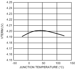
| VTERM_TOL | Battery charge termination voltage tolerance (selected in CHCTL Register (01)H Charger Control Register) | TJ = 25°C IPROG = 500 mA, ICHG = 50 mA |
–0.35% −0.5% −0.5% |
4.2 4.1 4.38 |
0.35% 0.5% 0.5% |
V |
| TJ = 0°C to 125°C IPROG = 500 mA, ICHG = 50 mA |
–1% –1.5% –1.5% |
4.2 4.1 4.38 |
1% 1.5% 1.5% |
V | ||
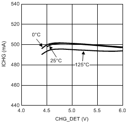
| ICHG_WA | Full-rate charging current from wall adapter input (see Full-Rate Charging Mode) | CHG_DET = 5.25 V VBATT = 3.6 V, IPROG = 500 mA |
450 | 500 | 550 | mA |
| ICHG_USB | Full-rate charging current from usbpwr input (see Full-Rate Charging Mode) | USB = 5 V, VBATT = 3.6 V IPROG = 500 mA, USB_ISEL = 800 mA |
450 | 500 | 550 | mA |
| USB = 5 V, VBATT = 3.6 V IPROG = 500 mA, USB_ISEL = 500 mA |
405 | 450 | 495 | mA | ||
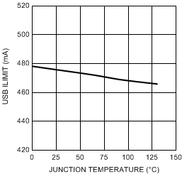
| USB ILIMIT | USB charge-current limit | USB_ISEL = 100 mA | 90 | 95 | 100 | mA |
| USB_ISEL = 500 mA | 450 | 475 | 500 | |||
| USB_ISEL = 800 mA | 720 | 760 | 800 | |||
| IPREQUAL | Pre-qualification current | VBATT = 2.5 V, wall-adapter charge current Percentage of programmed full-rate current |
8% | 10% | 12% | |
| VBATT = 2.5 V, USB charge current | 40 | 50 | 60 | mA | ||
| VFULL_RATE | Full-rate qualification threshold | VBATT rising, transition from pre-qualification to full-rate charging (standard) | 2.75 | 2.85 | 2.95 | V |
| VBATT rising, transition from pre-qualification to full-rate charging (AP version only) | 2.45 | 2.55 | 2.65 | |||
| VTH_H | Upper TS comparator limit | 2.82 | 2.87 | 2.93 | V | |
| VTH_L | Lower TS comparator limit | 45°C CHSPV Reg D3 = 0 | 0.315 | 0.33 | 0.345 | V |
| 50°C CHSPV Reg D3 = 1 | 0.255 | 0.27 | 0.285 | |||
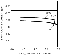
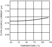
| ITSENSE | Battery temperature sense current | 7.75 | 8 | 8.25 | µA | |
| TREG | Regulated charger junction temperature | TJ = 25°C | 105 | 115 | 125 | °C |
(1) All voltages are with respect to the potential at the GND pin.
(2) Junction-to-ambient thermal resistance is highly application and board-layout dependent. In applications where high maximum power dissipation exists, special care must be paid to thermal dissipation issues in board design.
(3) Minimum and maximum limits are specified by design, test, or statistical analysis. Typical numbers are not ensured, but do represent the most likely norm.
(4) Low ESR Surface-Mount Ceramic Capacitors (MLCCs) are used in setting electrical characteristics.
7.8 Detection and Timing
Typical limits apply for TJ = 25°C; minimum and maximum limits apply for TJ = 0°C to 125°C, unless otherwise specified.| PARAMETER | TEST CONDITIONS | MIN | TYP | MAX | UNIT | |
|---|---|---|---|---|---|---|
| IEOC | End-of-charge current | IPROG = 500 mA 10% EOC setting |
40 | 50 | 60 | mA |
| IPROG = 500 mA 5% EOC setting |
20 | 25 | 30 | mA | ||
| VRESTART | Battery restart charging voltage | VTERM = 4.1 V | 3.82 | 3.9 | 3.94 | V |
| VTERM = 4.2 V | 3.94 | 4 | 4.06 | |||
| VTERM = 4.38 V | 4.14 | 4.2 | 4.26 | |||
7.9 Output Electrical Characteristics: CHG, STAT
Unless otherwise noted, VDD = 5 V, VBATT = 3.6 V. CBATT = 4.7 µF, CCHG_DET = 10 µF. Typical limits apply for TJ = 25°C; minimum and maximum limits apply for TJ = 0°C to 125°C, unless otherwise specified.(1)(2)(3)(4)| PARAMETER | TEST CONDITIONS | MIN | TYP | MAX | UNIT | |
|---|---|---|---|---|---|---|
| ILED | Output high level | VLED = 2 V CHSPV Register (02)h bit 5 = 1 (standard) |
4 | 5 | 6 | mA |
| VLED = 2 V CHSPV Register (02)h bit 5 = 1 (AP version only) |
0.75 | 1 | 1.25 | |||
| ILED | Output high level | VLED = 2 V CHSPV Register (02)h bit 5 = 0 (standard) |
8 | 10 | 12 | mA |
| VLED = 2 V CHSPV Register (02)h bit 5 = 0 (AP version only) |
1.6 | 2 | 2.4 | |||
| ILEAKAGE | Leakage current | VLED = 1.5 V, LED off | 0.1 | 5 | µA | |
| LEDFREQ | Blinking frequency | 0.8 | 1 | 1.2 | Hz | |
(1) All voltages are with respect to the potential at the GND pin.
(2) Junction-to-ambient thermal resistance is highly application and board-layout dependent. In applications where high maximum power dissipation exists, special care must be paid to thermal dissipation issues in board design.
(3) Minimum and maximum limits are specified by design, test, or statistical analysis. Typical numbers are not ensured, but do represent the most likely norm.
(4) Low ESR Surface-Mount Ceramic Capacitors (MLCCs) are used in setting electrical characteristics.
7.10 Output Electrical Characteristics: NRST, IRQB, ONSTAT
Unless otherwise noted, VDD = 5 V, VBATT = 3.6 V, CBATT = 4.7 µF, CCHG_DET = 10 µF. Minimum and maximum limits apply over the entire junction temperature range for operation, TJ = 0°C to 125°C.(1)(2)(3)(4)| PARAMETER | TEST CONDITIONS | MIN | TYP | MAX | UNIT | |
|---|---|---|---|---|---|---|
| VOL | Output low level | IOL = 4 mA | 0.4 | V | ||
| ILEAKAGE | Leakage current | VDD = 2.5 V, output logic high | –1 | 1 | µA | |
(1) All voltages are with respect to the potential at the GND pin.
(2) Junction-to-ambient thermal resistance is highly application and board-layout dependent. In applications where high maximum power dissipation exists, special care must be paid to thermal dissipation issues in board design.
(3) Minimum and maximum limits are specified by design, test, or statistical analysis.
(4) Low ESR Surface-Mount Ceramic Capacitors (MLCCs) are used in setting electrical characteristics.
7.11 Input Electrical Characteristics: USBSUSP, USBISEL
Unless otherwise noted, VUSB = 5 V, VBATT = 3.6 V, CBATT = 4.7 µF, CCHG_DET = 10 µF. Minimum and maximum limits apply over the entire junction temperature range for operation, TJ = 0°C to 125°C.(1)(2)(3)(4)(5)| PARAMETER | TEST CONDITIONS | MIN | TYP | MAX | UNIT | |
|---|---|---|---|---|---|---|
| VIL | Input low level | 0.3 × VUSB | V | |||
| VIH | Input high level | 0.7 × VUSB | V | |||
| ILEAKAGE | Input leakage | −1 | 1 | µA | ||
(1) LDO2EN, BUCK1EN, and USBSUSP have weak internal pulldowns while pins POWERACK, ONOFF do not have weak pulldowns.
(2) All voltages are with respect to the potential at the GND pin.
(3) Junction-to-ambient thermal resistance is highly application and board-layout dependent. In applications where high maximum power dissipation exists, special care must be paid to thermal dissipation issues in board design.
(4) Minimum and maximum limits are specified by design, test, or statistical analysis.
(5) Low ESR Surface-Mount Ceramic Capacitors (MLCCs) are used in setting electrical characteristics.
7.12 Input Electrical Characteristics: POWERACK, ONOFF, LDO2EN, BUCK1EN
Unless otherwise noted, VDD = 5 V, VBATT = 3.6 V, CBATT = 4.7 µF, CCHG_IN = 10 µF. Minimum and maximum limits apply over the entire junction temperature range for operation, TJ = 0°C to 125°C.(1)(2)(3)(4)(5)| PARAMETER | TEST CONDITIONS | MIN | TYP | MAX | UNIT | |
|---|---|---|---|---|---|---|
| VIL | Input low level | 0.4 | V | |||
| VIH | Input high level | 1.4 | V | |||
| ILEAKAGE | Input leakage | –1 | 1 | µA | ||
(1) LDO2EN, BUCK1EN, and USBSUSP have weak internal pulldowns, while pins POWERACK, ONOFF do not have this.
(2) All voltages are with respect to the potential at the GND pin.
(3) Junction-to-ambient thermal resistance is highly application and board-layout dependent. In applications where high maximum power dissipation exists, special care must be paid to thermal dissipation issues in board design.
(4) Minimum and maximum limits are specified by design, test, or statistical analysis.
(5) Low ESR Surface-Mount Ceramic Capacitors (MLCCs) are used in setting electrical characteristics.
7.13 Electrical Characteristics: LDO1 Low Dropout Linear Regulators
Unless otherwise noted, VIN1 = 3.6 V, IMAX = 150 mA, VOUT = default value, CVDD = 10 µF, CLDO1 = 1 µF, ESR = 5 mΩ – 500 mΩ, CVREFH = 100 nF. Typical limits apply for TJ = 25°C; minimum and maximum limits apply for TJ = 0°C to 125°C, unless otherwise specified.| PARAMETER | TEST CONDITIONS | MIN | TYP | MAX | UNIT | |
|---|---|---|---|---|---|---|
| VIN1 | Operational voltage | 2.5 | 6 | V | ||
| VOUT Range | Output voltage programming range | TJ = 25°C 1.2 V to 3.3 V in 100-mV steps |
1.2 | 3.3 | V | |
| VOUT Accuracy | Output voltage accuracy | 1 mA ≤ IOUT ≤ IMAX over full line and load regulation. VOUT = default value |
–3% | 3% | ||
| ΔVOUT | Line regulation | VIN = (VOUT + 500 mV) to 5.5 V Load current = IMAX |
3 | mV | ||
| Load regulation | VIN = 3.6 V, Load current = 1 mA to IMAX |
10 | mV | |||
| ISC | Short-circuit current limit | VOUT = 0 V | 600 | 750 | mA | |
| VIN – VOUT | Dropout voltage | Load current = IMAX | 60 | 150 | mV | |
| PSRR | Power supply ripple rejection | F = 10 kHz, load current = IMAX | 30 | dB | ||
| RSHUNT | LDO output impedance | LDO disabled, VOUT = default value | 200 | Ω | ||
7.14 Electrical Characteristics: LDO2 Low Dropout Linear Regulator
Unless otherwise noted VIN1 = 3.6V, IMAX = 150 mA, VOUT = default value, CVDD = 10 µF, CLDO2 = 1 µF, ESR = 5 mΩ to 500 mΩ, CVREFH = 100 nF. Typical limits apply for TJ = 25°C; minimum and maximum limits apply for TJ = 0°C to 125°C, unless otherwise specified.| PARAMETER | TEST CONDITIONS | MIN | TYP | MAX | UNIT | |
|---|---|---|---|---|---|---|
| VIN2 | Operational voltage | 2.5 | 6 | V | ||
| VOUT range | Output voltage programming range | TA = 25°C 1.3 V to 3.3 V in 100-mV steps |
1.3 | 3.3 | V | |
| VOUT accuracy | Output voltage accuracy (default VOUT) |
1 mA ≤ IOUT ≤ IMAX over full line and load regulation | –3% | 3% | ||
| ΔVOUT | Line regulation | VIN = (VOUT + 500 mV) to 5.5 V, Load current = IMAX |
3 | mV | ||
| Load regulation | VIN = 3.6 V, Load current = 1 mA to IMAX |
10 | mV | |||
| ISC | Short-circuit current limit | VOUT = 0 V | 600 | 750 | mA | |
| VIN – VOUT | Dropout voltage | Load current = IMAX | 60 | 150 | mV | |
| PSRR | Power supply ripple rejection | F = 1 kHz, load current = IMAX | 50 | dB | ||
| F = 10 kHz, load current = IMAX | 35 | |||||
| eN | Analog supply output noise voltage | 10 Hz < F < 100 kHz | 50 | µVRMS | ||
| RSHUNT | LDO output impedance | LDO disabled, VOUT = default value | 200 | Ω | ||
7.15 Electrical Characteristics: Buck1 Converter
Unless otherwise noted, VIN2 = 3.6 V, VOUT = default value, CVIN2 = 10 µF, CSW1 = 10 µF, LSW1 = 2.2 µH. Typical limits apply for TJ = 25°C; minimum and maximum limits apply for TJ = 0°C to 125°C, unless otherwise specified. Modulation mode is PWM mode with automatic switch to PFM at light loads.| PARAMETER | TEST CONDITIONS | MIN | TYP | MAX | UNIT | |
|---|---|---|---|---|---|---|
| VIN2 | Input voltage | 2.7 | 6 | V | ||
| VOUT range | Output voltage programming range | TJ = 25°C 0.8 V to 2 V in 50-mV Steps |
0.8 | 2 | V | |
| ΔVOUT | Static output voltage tolerance | IOUT = 200 mA including line and load regulation | –3% | 3% | ||
| Line regulation | IOUT = 10 mA VIN2 = 2.5 V − VDD |
0.2 | %/V | |||
| Load regulation | 100 mA < IOUT < 300 mA | 0.002 | %/mA | |||
| IOUT | Continuous output current | 600 | mA | |||
| Peak output current limit | 850 | 1000 | 1150 | mA | ||
| IPFM | Maximum ILOAD, PFM mode | 75 | mA | |||
| IQ | Quiescent current | IOUT = 0 mA | 30 | 90 | µA | |
| BUCK1 disabled | 1 | |||||
| FOSC | Internal oscillator frequency | PWM mode | 2 | MHz | ||
| η | Peak efficiency | 90% | ||||
| TON | Turnon time | To 95% level(1) | 1 | ms | ||
(1) This specification is ensured by design.
7.16 Electrical Characteristics: Buck2 Converter
Unless otherwise noted, VIN3 = 3.6 V, VOUT = default value, CVIN3 = 10 µF, CSW1 = 10 µF, LSW2 = 2.2 µH. Typical limits apply for TJ = 25°C; minimum and maximum limits apply for TJ = 0°C to 125°C, unless otherwise specified. Modulation mode is PWM mode with automatic switch to PFM at light loads.| PARAMETER | TEST CONDITIONS | MIN | TYP | MAX | UNIT | |
|---|---|---|---|---|---|---|
| VIN3 | Input voltage | 2.7 | 6 | V | ||
| VOUT Range | Output voltage programming range | 1.8 V – 3.3 V in 100-mV steps | 0.8 | 2 | V | |
| ΔVOUT | Static output voltage tolerance | IOUT = 200 mA including line and load regulation | –3% | 3% | ||
| Line regulation | IOUT = 10 mA VIN3 = 2.5 V − VDD |
0.2 | %/V | |||
| Load regulation | 100 mA < IOUT < 300 mA | 0.002 | %/mA | |||
| IOUT | Continuous output current | 600 | mA | |||
| Peak output current limit | 850 | 1000 | 1150 | mA | ||
| IPFM | Maximum ILOAD, PFM mode | 75 | mA | |||
| IQ | Quiescent current | IOUT = 0 mA | 30 | 90 | µA | |
| Buck2 disabled | 1 | |||||
| FOSC | Internal oscillator frequency | PWM mode | 2 | MHz | ||
| η | Peak efficiency | 90% | ||||
| TON | Turnon time | To 95% level(1) | 1 | ms | ||
(1) This specification is ensured by design..
7.17 Electrical Characteristics: Buck-Boost
Unless otherwise noted, VIN4 = 3.6 V, CVIN4 = 10 µF, CBB = 22 µF, LBB = 2.2 µH. Typical limits apply for TJ = 25°C; minimum and maximum limits apply for TJ = 0°C to 125°C, unless otherwise specified. Modulation mode is PWM mode with automatic switch to PFM at light loads.| PARAMETER | TEST CONDITIONS | MIN | TYP | MAX | UNIT | |
|---|---|---|---|---|---|---|
| VIN4 | Input voltage | IOUTMAX = 1000 mA | 2.9 | 5.7 | V | |
| IOUTMAX = 800 mA | 2.7 | 5.7 | V | |||
| VOUT Range | Output voltage programming range | TJ = 25°C 1.80 V to 3.30 V in 50-mV steps |
1.8 | 3.3 | V | |
| ΔVOUT | Static output voltage tolerance | IOUT = 0 mA to 1000 mA including line and load regulation | –4% | 4% | ||
| Line regulation | IOUT = 10 mA | 0.2 | %/V | |||
| Load regulation | 100 mA < IOUT < 1000 mA | 0.0016 | %/mA | |||
| IOUT | Continuous output current | 1000 | mA | |||
| Peak inductor current limit | VOUT = 3.3 V 1-A load at VIN = 2.7 V |
1800 | 2400 | mA | ||
| IPFM | Maximum ILOAD, PFM mode | 75 | mA | |||
| IQ | Quiescent current | IOUT = 0 mA PFM no switching | 80 | µA | ||
| Buck-Boost disabled | 1 | |||||
| FOSC | Internal oscillator frequency | PWM mode | 2 | MHz | ||
| η | Peak efficiency | 93% | ||||
| TON | Turnon time | To 95% level(1) | 1 | ms | ||
(1) This specification is ensured by design.
7.18 Electrical Characteristics: ADC
All limits apply for TJ = 25°C unless otherwise specified.| PARAMETER | TEST CONDITIONS | MIN | TYP | MAX | UNIT | |
|---|---|---|---|---|---|---|
| VREF | Reference voltage | TJ = 25°C | 1.22 | 1.225 | 1.23 | V |
| TJ = 0°C to 125°C | 1.2 | 1.225 | 1.23 | V | ||
| INL | Core ADC integral non-linearity | VREF = 1.225(1) | –1 | 1 | LSB | |
| DNL | Core ADC differential non-linearity | VREF = 1.225(1) | –0.5 | 0.5 | LSB | |
| VGP_IN | General purpose ADC input voltage range | VREF | 2 × VREF | V | ||
| VBATT, RANGE 0 | Battery maximum voltage scalar output | VBATT = 3.5 V | 2.435 | 2.45 | 2.465 | V |
| Battery minimum voltage scalar output | VBATT = 2.6 V | 1.217 | 1.225 | 1.232 | V | |
| VBATT, RANGE 1 | Battery maximum voltage scalar output | VBATT = 4.4 V | 2.435 | 2.45 | 2.465 | V |
| Battery minimum voltage scalar output | VREF = 2.6 V | 1.217 | 1.225 | 1.232 | V | |
| VISENSE , RANGE 0 | ISENSE maximum voltage scalar output | VISENSE = 0.6463 V ICHG = 0.605 A, RSENSE = 4.64 kΩ |
2.373 | 2.45 | 2.519 | V |
| ISENSE minimum voltage scalar output | VISENSE = 0 V ICHG = 0 A, RSENSE = 4.64 kΩ |
1.186 | 1.225 | 1.260 | V | |
| VISENSE, RANGE 1 | ISENSE maximum voltage scalar output | VISENSE = 1.175 V ICHG = 1.1 A, RSENSE = 4.64 kΩ |
2.373 | 2.45 | 2.519 | V |
| ISENSE minimum voltage scalar output | VISENSE = 0 V ICHG = 0 A, RSENSE = 4.64 kΩ |
1.186 | 1.225 | 1.26 | V | |
| ADC1 and ADC2MIN | ADC1 and ADC2 minimum voltage scalar output | VREFH = 1.225 V | 1.218 | 1.225 | 1.23 | V |
| ADC1 and ADC2MAX | ADC1 and ADC2 maximum voltage scalar output | VREFH = 1.225 V | 2.436 | 2.45 | 2.46 | V |
| tCONV | Conversion time(1) | 5 | ms | |||
| tWARM | Warm-up time | 2 | ms | |||
(1) This specification is ensured by design.
7.19 I2C Timing Requirements
Unless otherwise noted, VDDIO = 3.6 V and minimum and maximum limits apply for TJ = 0°C to 125°C.(1)| MIN | NOM | MAX | UNIT | ||
|---|---|---|---|---|---|
| FCLK | Clock frequency | 400 | kHz | ||
| tBF | Bus-free time between START and STOP | 1.3 | µs | ||
| tHOLD | Hold time repeated START condition | 0.6 | µs | ||
| tCLK-LP | CLK low period | 1.3 | µs | ||
| tCLK-HP | CLK high period | 0.6 | µs | ||
| tSU | Set-up time repeated START condition | 0.6 | µs | ||
| tDATA-HOLD | Data hold time | 0 | µs | ||
| tDATA-SU | Data set-up time | 100 | ns | ||
| tSU | Set-up time for STOP condition | 0.6 | µs | ||
| tTRANS | Maximum pulse width of spikes that must be suppressed by the input filter of both data and CLK signals TJ = 25°C |
50 | µs | ||
(1) These specifications are ensured by design.
7.20 USB Timing Requirements
Nominal limits apply for TJ = 25°C; minimum and maximum limits apply for TJ = 0°C to 125°C, unless otherwise specified.| MIN | NOM | MAX | UNIT | ||
|---|---|---|---|---|---|
| TCHG_IN | Deglitch adapter insertion | 28 | 32 | 36 | ms |
| TUSB | Deglitch USB power insertion | 28 | 32 | 36 | ms |
| TPQ_FULL | Deglitch time for pre-qualification to full-rate charge transition | 8 | 10 | 12 | ms |
| TFULL_PQ | Deglitch time for full-rate to pre-qualification transition | 8 | 10 | 12 | ms |
| TBATTLOWF | Deglitch time for VBATT falling below VBATTLOW threshold | 4 | 5 | 6 | ms |
| TBATTLOWR | Deglitch time for VBATT rising above VBATTLOW threshold | 4 | 5 | 6 | ms |
| TBATTEMP | Deglitch time for recovery from battery temperature fault | 8 | 10 | 12 | ms |
| TONOFF_F | Deglitching on falling edge of ONOFF pin | 28 | 32 | 36 | ms |
| TONOFF_R | Deglitching on rising edge of ONOFF pin | 28 | 32 | 36 | ms |
| TRESTART | Deglitching on falling VBATT crossing VRESTART | 8 | 10 | 12 | ms |
| TCCCV | Deglitching of CC→CV charging transition | 8 | 10 | 12 | ms |
| TCVEOC | Deglitching of CV→EOC (End of Charge) | 8 | 10 | 12 | ms |
| TPOWERACK | Deglitching of POWERACK pin | 4 | 5 | 6 | ms |
| TTSHD | Deglitching of thermal shutdown | 2 | ms | ||
| TTOPOFF | Topoff timer | 17 | 21 | 25 | min |
| T10HR | 10-hour safety timer | 9 | 10 | 11 | hours |
| T1HR | 1-hour prequalification safety timer | 0.9 | 1 | 1.1 | hour |
7.21 Typical Characteristics
TA = 25°C unless otherwise noted7.21.1 Battery-Charger Characteristics

| Prequal IPROG = 500 mA | CHG_DET = 5 V | |
| VBATT = 3.5 V, CC |

| VBATT = 3.75 V, Prequal | CHG_DET = 5 V |
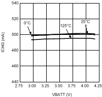
| CHG_DET = 5 V | CC |
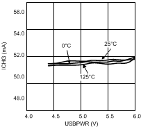
| VBATT = 2.5 V Prequal | ||
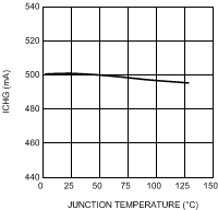
| VBATT = 3.75 V, CC | CHG_DET = 5 V |
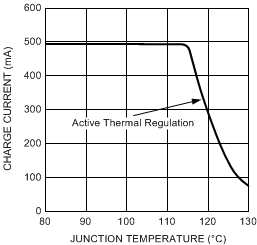
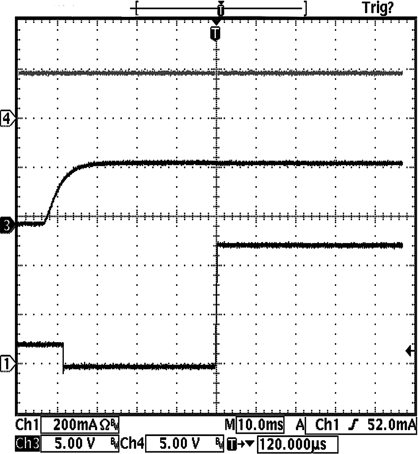
| Ch1 = Charge Current (mA) | Ch4 = USBPWR (V) | |
| Ch3 = CHG_DET (V) | ||
7.21.2 LDO Characteristics

| VIN = 4.3 V | VOUT = 3.3 V | Load = 100 mA |
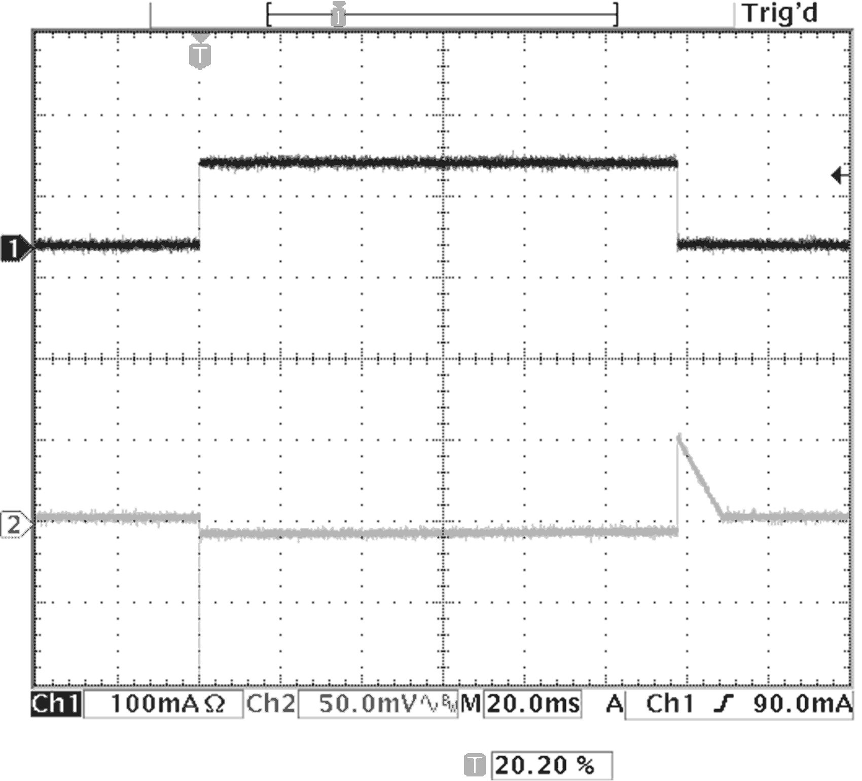
| VIN = 3.6 V | VOUT = 3.3 V | Load = 0 to 100 mA |
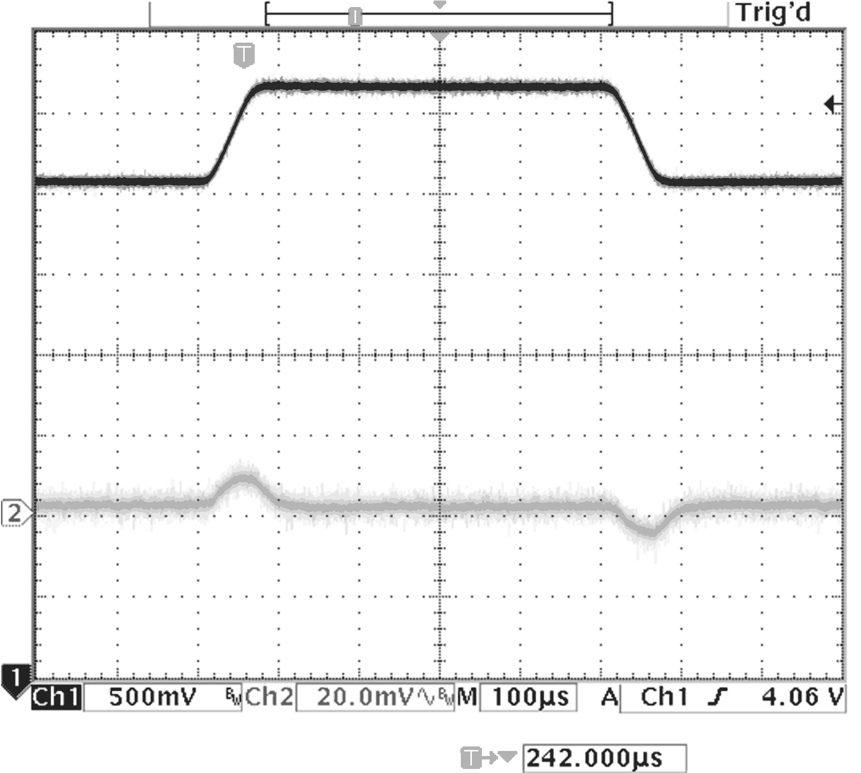
| VIN = 3.6 to 4.5 V | VOUT = 3.3 V | Load = 150 mA |
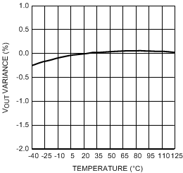
| VIN = 4.3 V | VOUT = 1.8 V | Load = 100 mA |
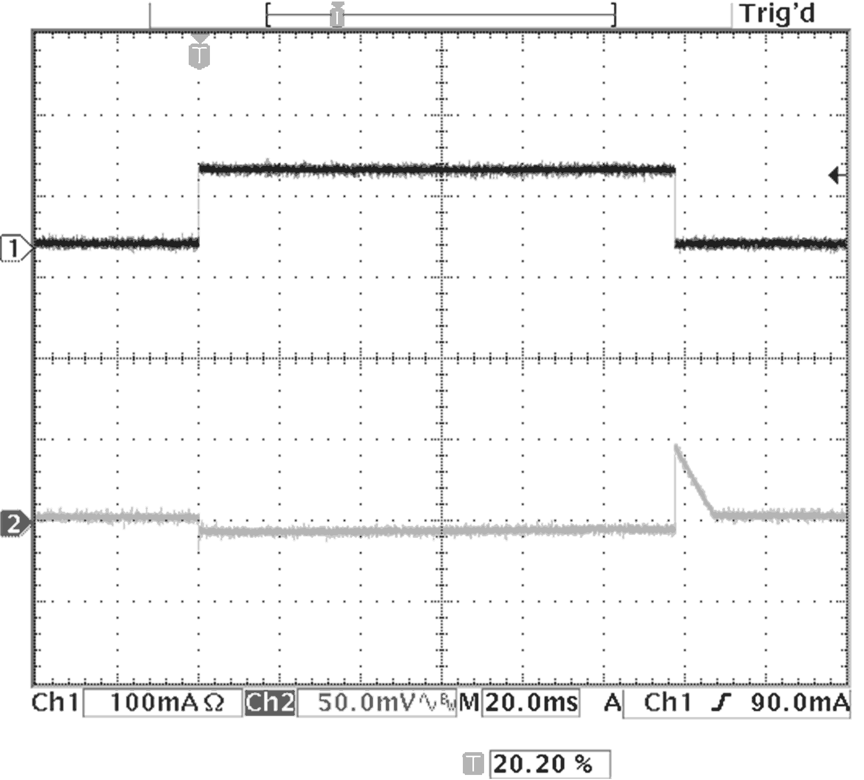
| VIN = 3.6 V | VOUT = 1.8 V | Load = 0 to 100 mA |
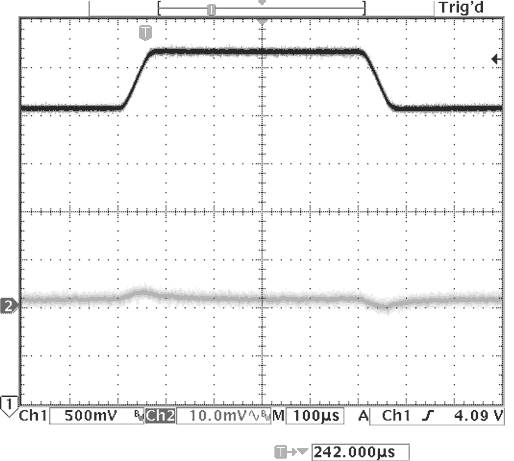
| VIN = 3 to 4.2 V | VOUT = 1.8 V | Load = 150 mA |
7.21.3 Buck Characteristics
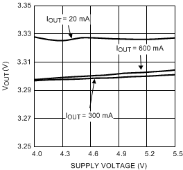
| VOUT = 3.3 V |

| VOUT = 1.2 V |
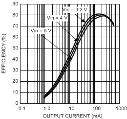
| VOUT = 1.2 V | L = 2.2 µH | Forced PWM Mode |

| VOUT = 1.2 V | L = 2.2 µH | PFM-to-PWM Mode |
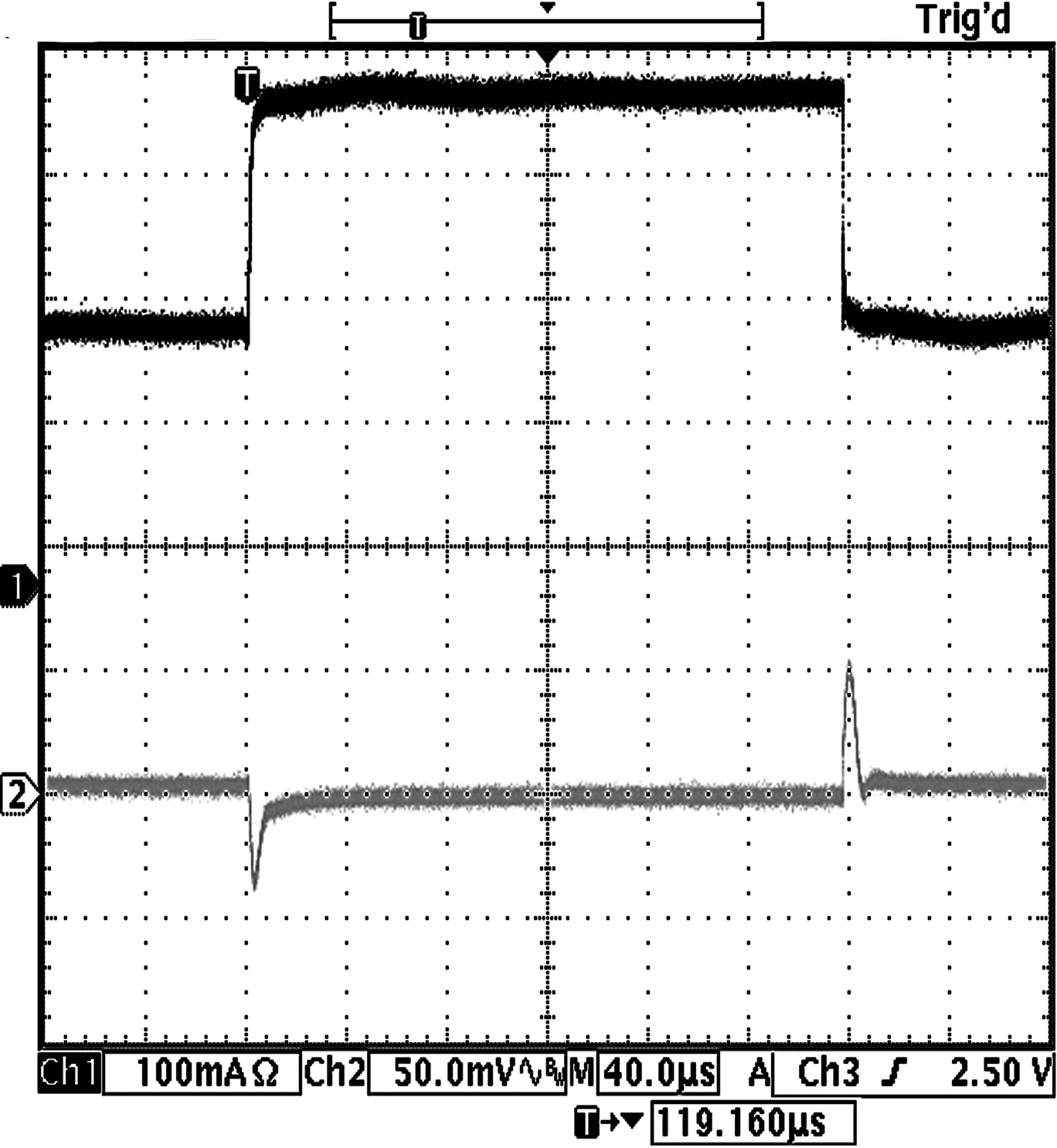
| VIN = 4.2 V | VOUT = 1.2 V | Load = 200 to 400 mA |
| PWM Mode |
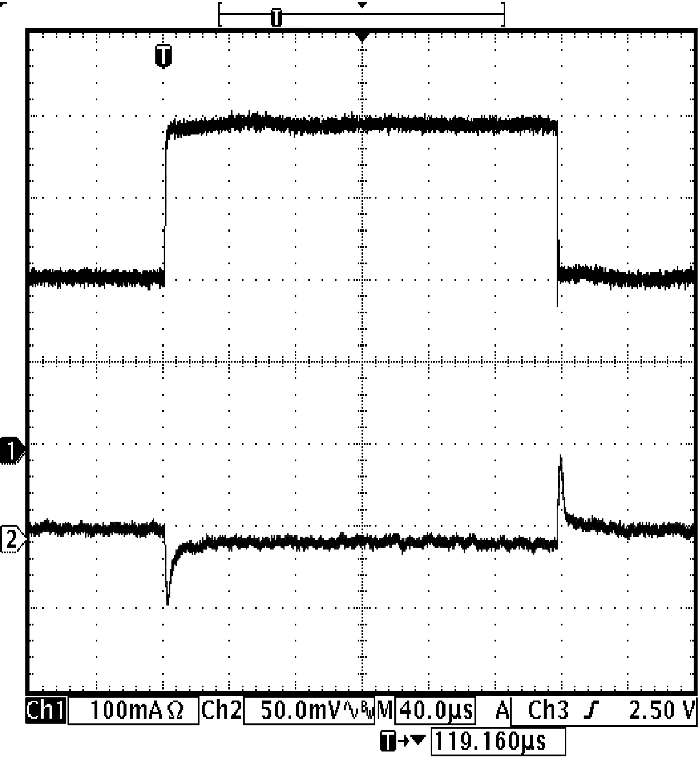
| VIN = 4.2 V | VOUT = 3.3 V | Load = 0 to 400 mA |
| PWM Mode |
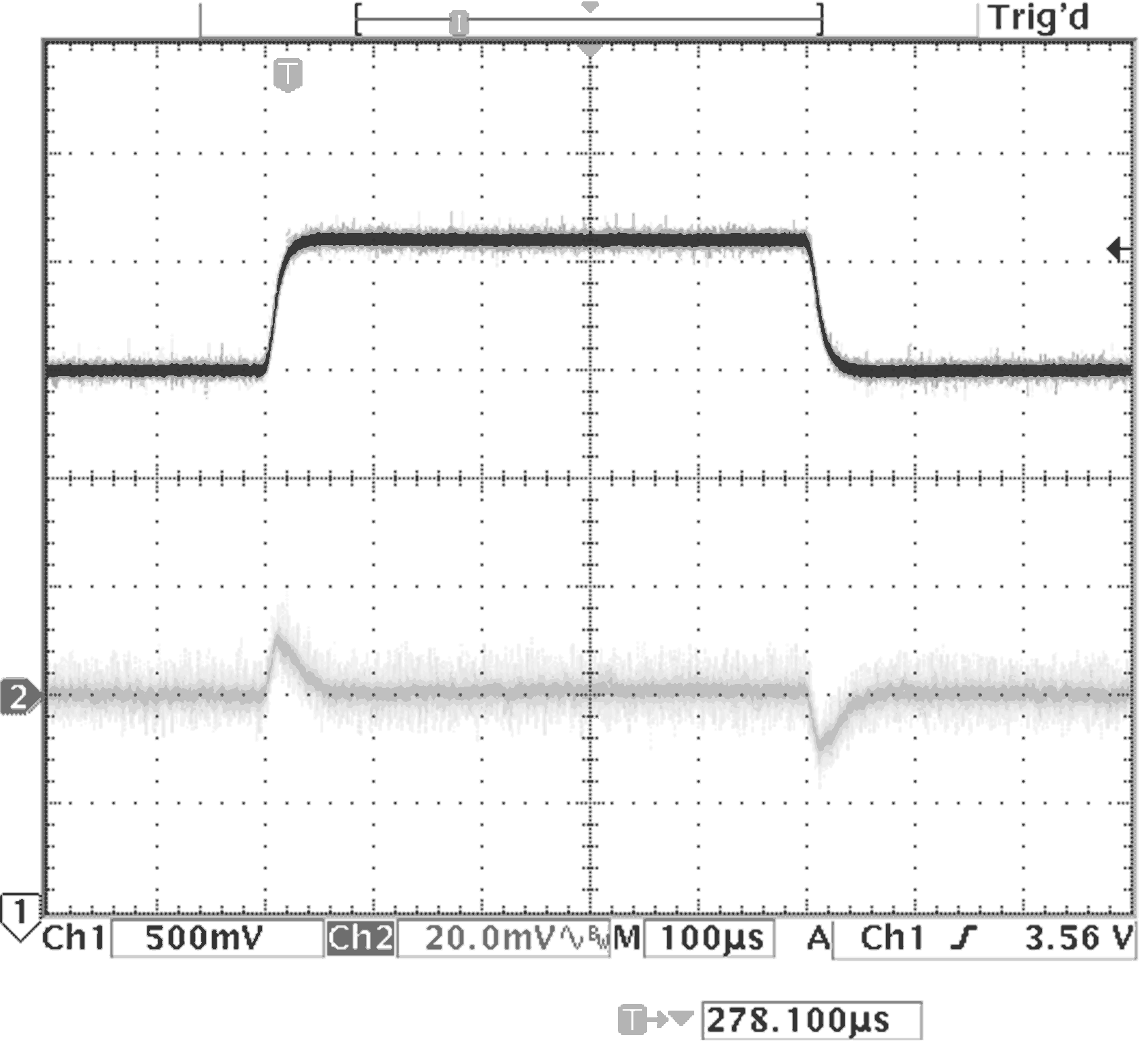
| VIN = 3 to 3.6 V | VOUT = 1.2 V | Load = 250 mA |
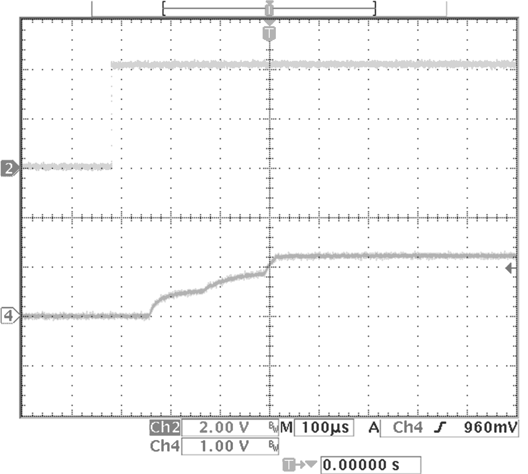
| VOUT = 1.8 V | Load = 30 mA |

| VOUT = 1.8 V | Load = 30 mA |
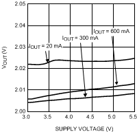
| VOUT = 2 V |

| VOUT = 0.8 V |
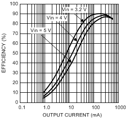
| VOUT = 2 V | L = 2.2 µH | Forced PWM Mode |
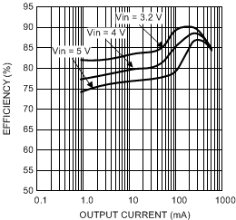
| VOUT = 2 V | L = 2.2 µH | PFM-to-PWM Mode |
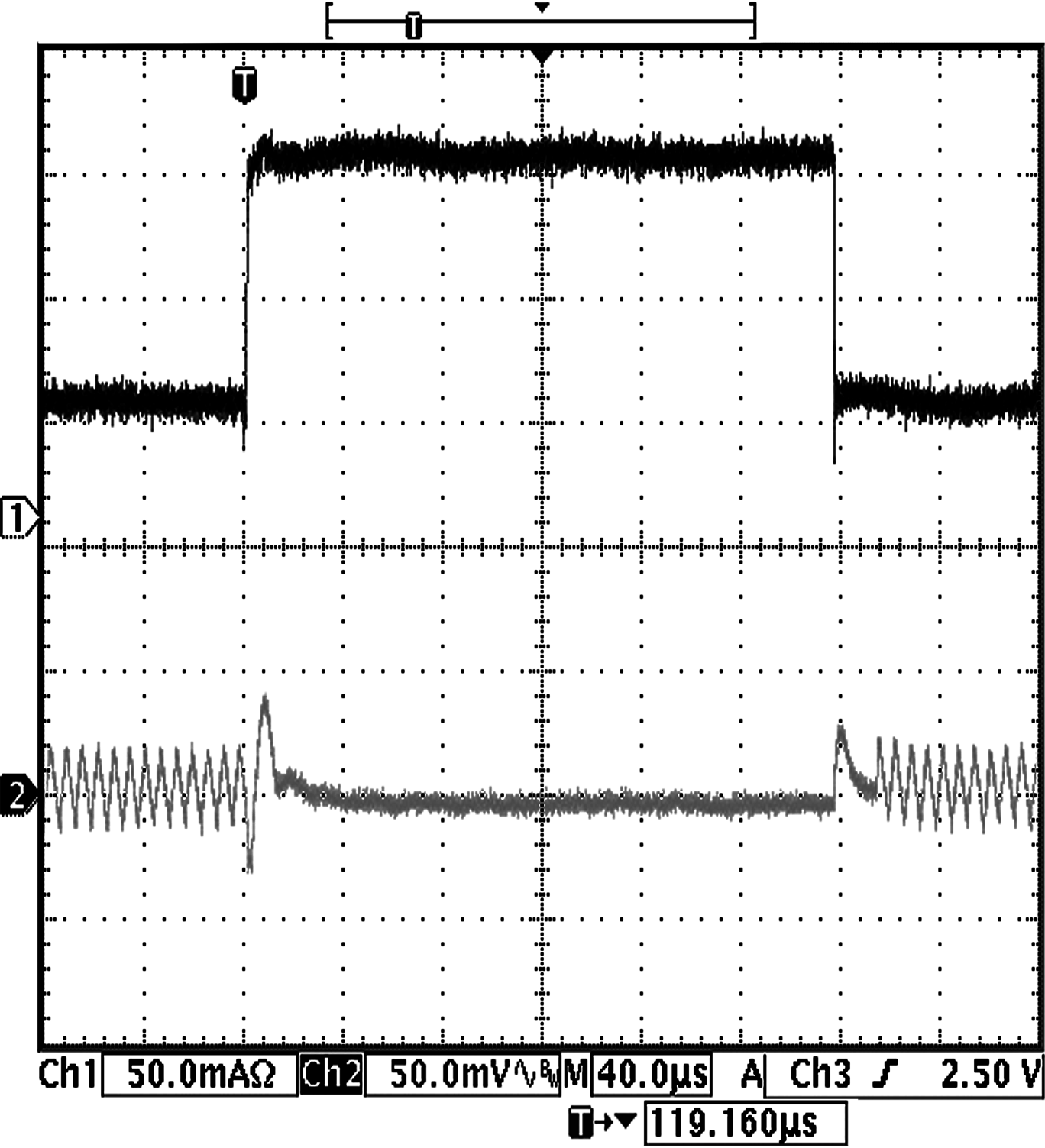
| VIN = 4.2 V | VOUT = 1.2 V | Load = 50 to 150 mA |
| PFM-to-PWM Mode | ||
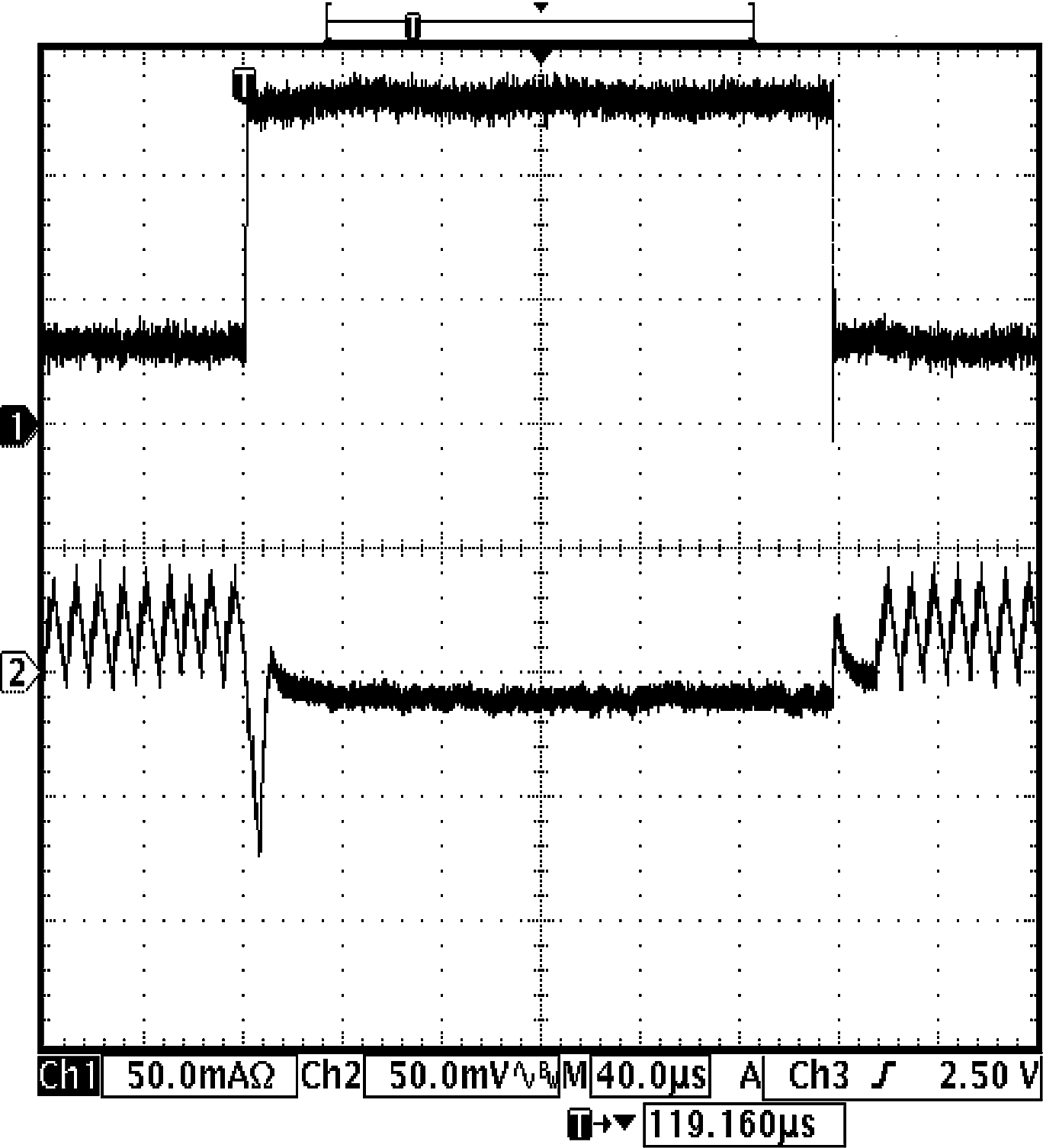
| VIN = 4.2 V | VOUT = 3.3 V | Load = 50 to 150 mA |
| PFM-to_PWM Mode | ||

| VIN = 3 to 3.6 V | VOUT = 3.3 V | Load = 250 mA |

| VOUT = 3.3 V | Load = 30 mA |
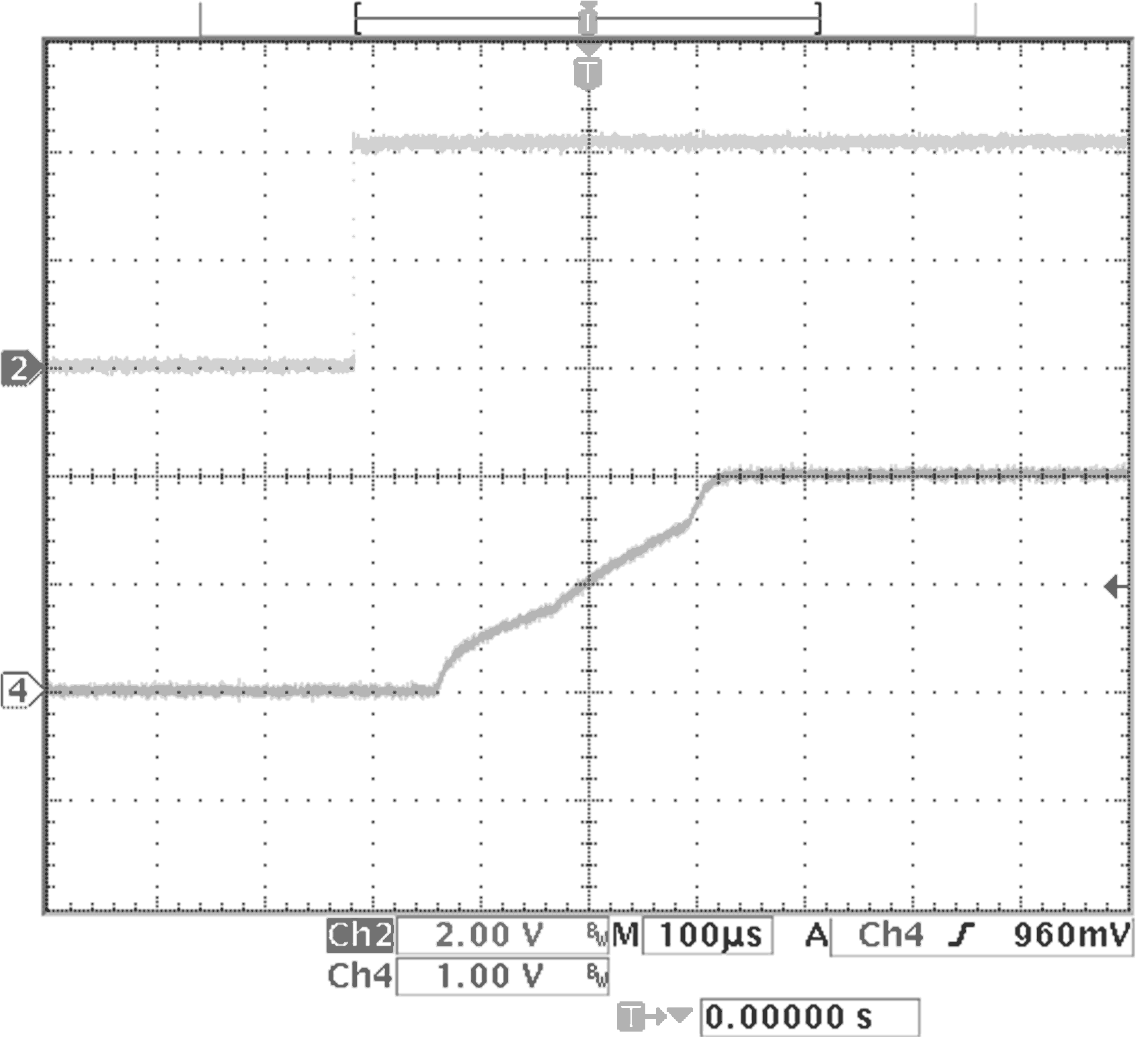
| VOUT = 3.3 V | Load = 30 mA |
7.21.4 Buck-Boost Characteristics
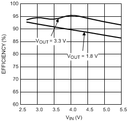
| ILOAD= 100 mA |
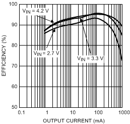
| VOUT = 3.3 V |
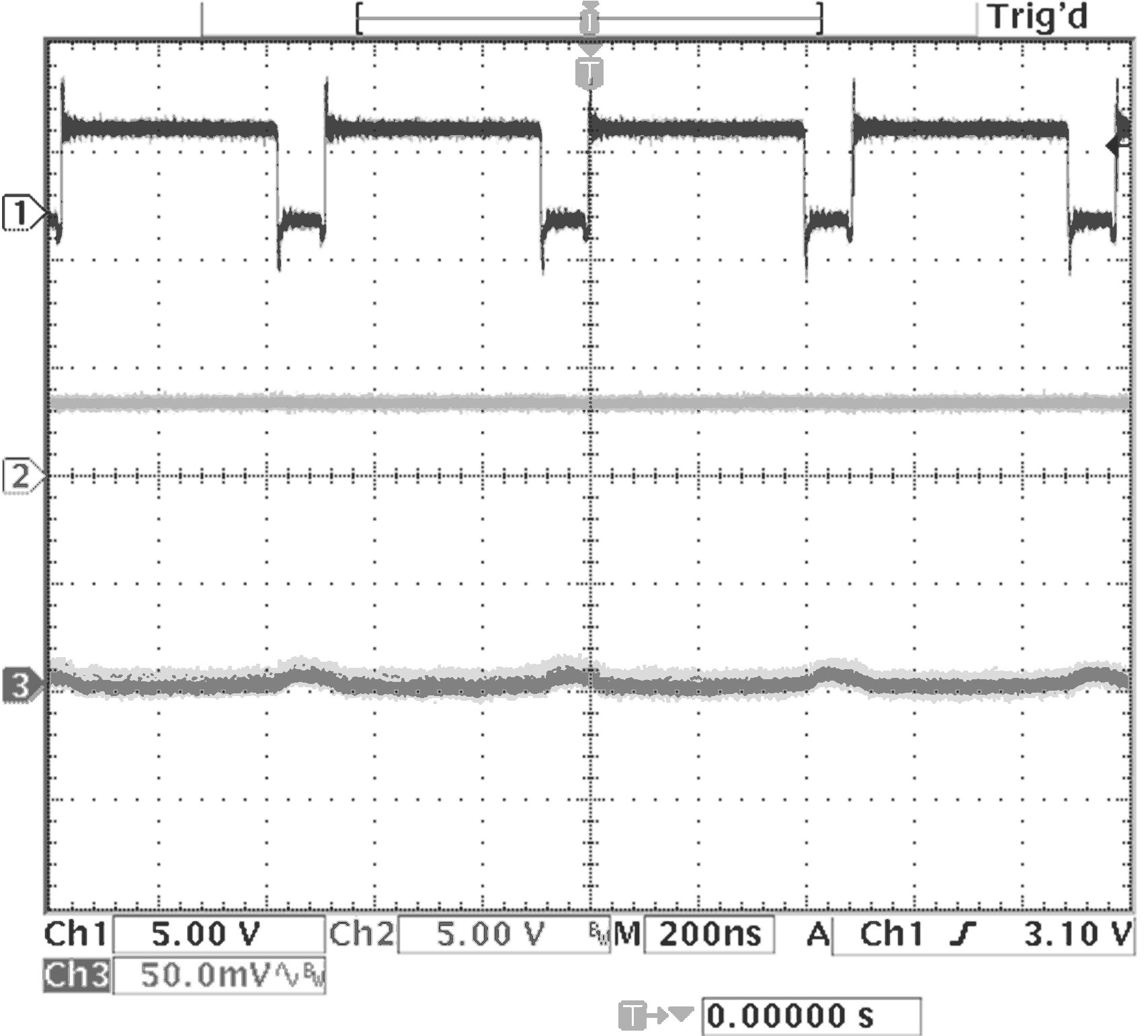
| VIN = 4.2 V | VOUT = 3.3 V | ILOAD = 250 mA |
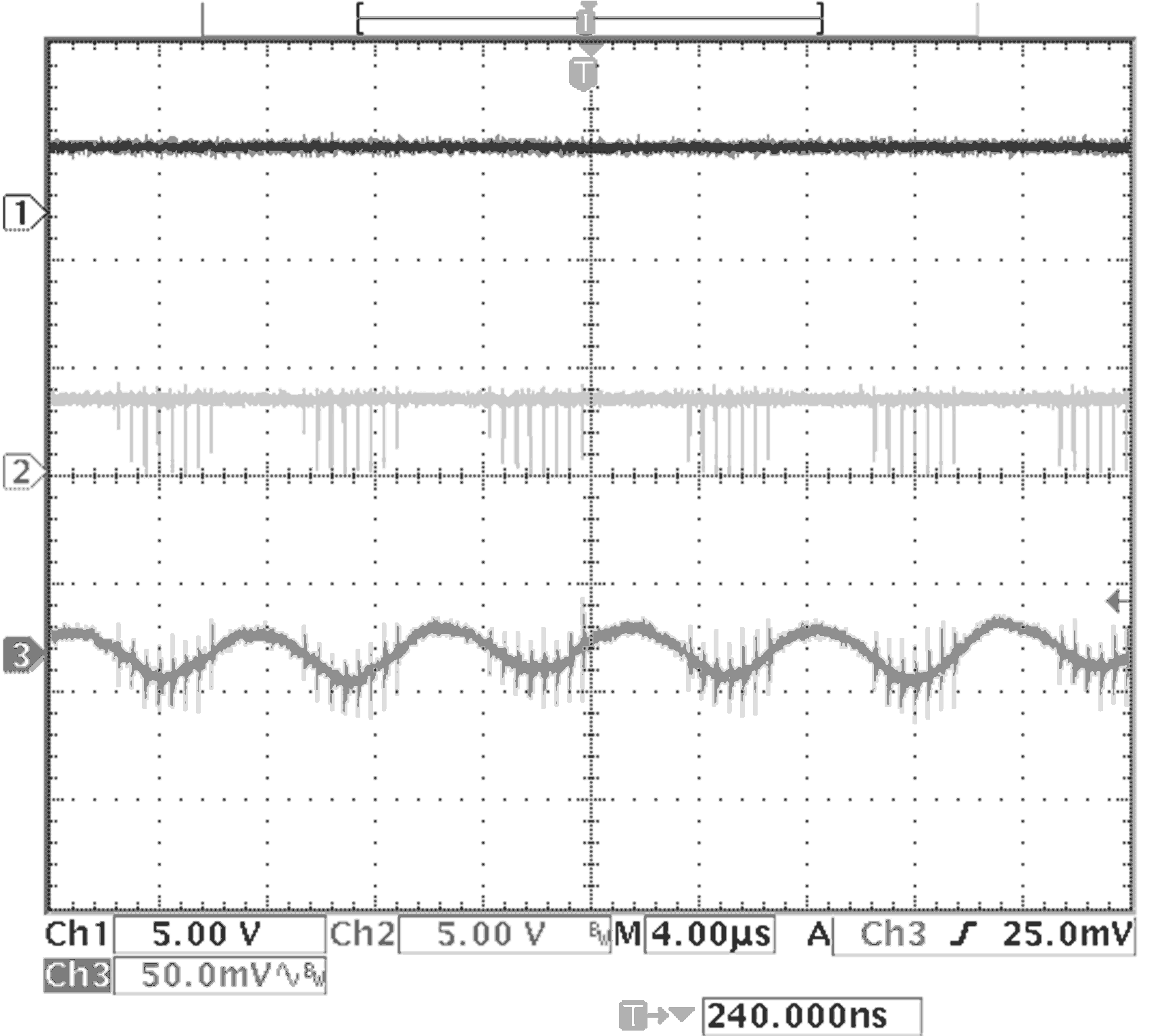
| VIN = 3.35 V | VOUT = 3.3 V | ILOAD = 250 mA |
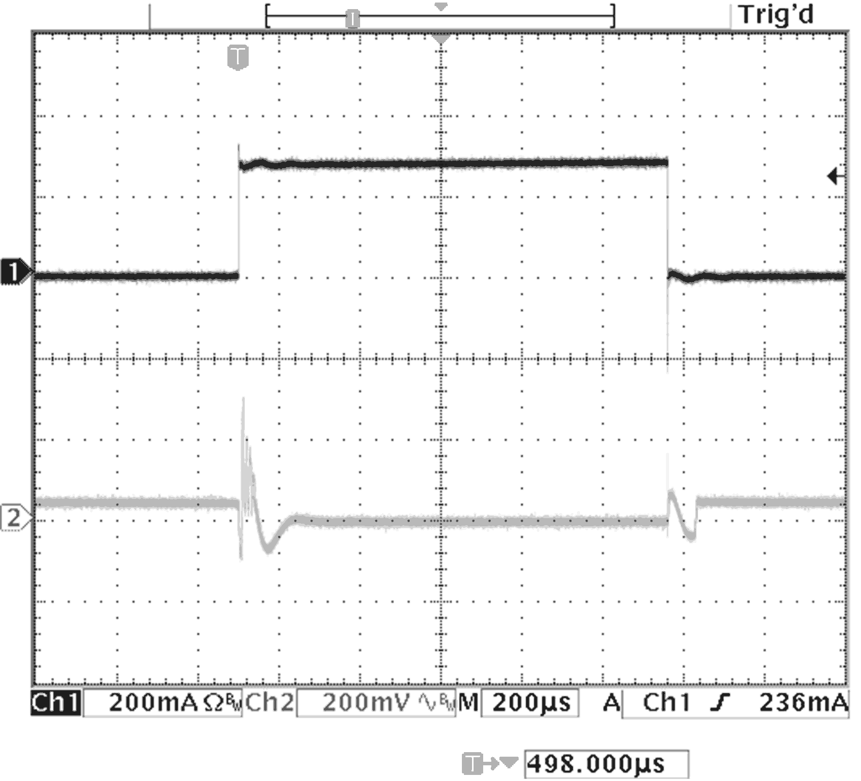
| VIN = 4.2 V | VOUT = 3.3 V | ILOAD = 0 to 500 mA |
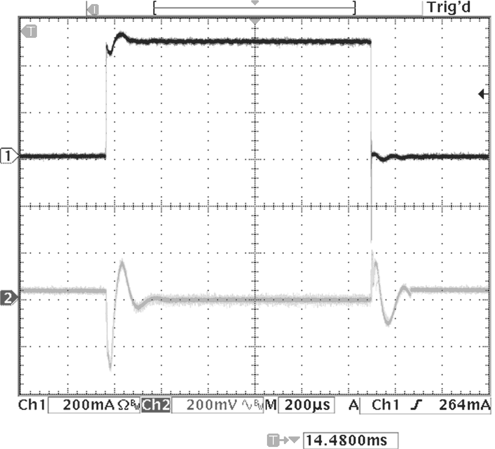
| VIN = 2.7 V | VOUT = 3.3 V | ILOAD = 0 to 500 mA |
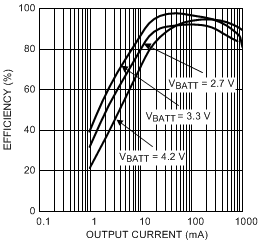
| VOUT = 3.3 V |
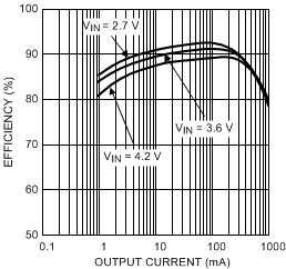
| VOUT = 1.8 V |
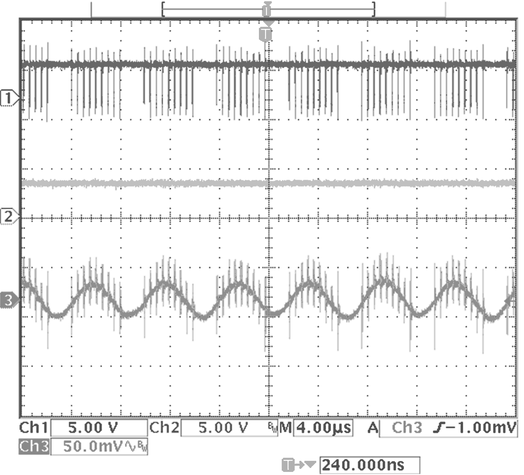
| VIN = 3.6 V | VOUT = 3.3 V | ILOAD = 250 mA |
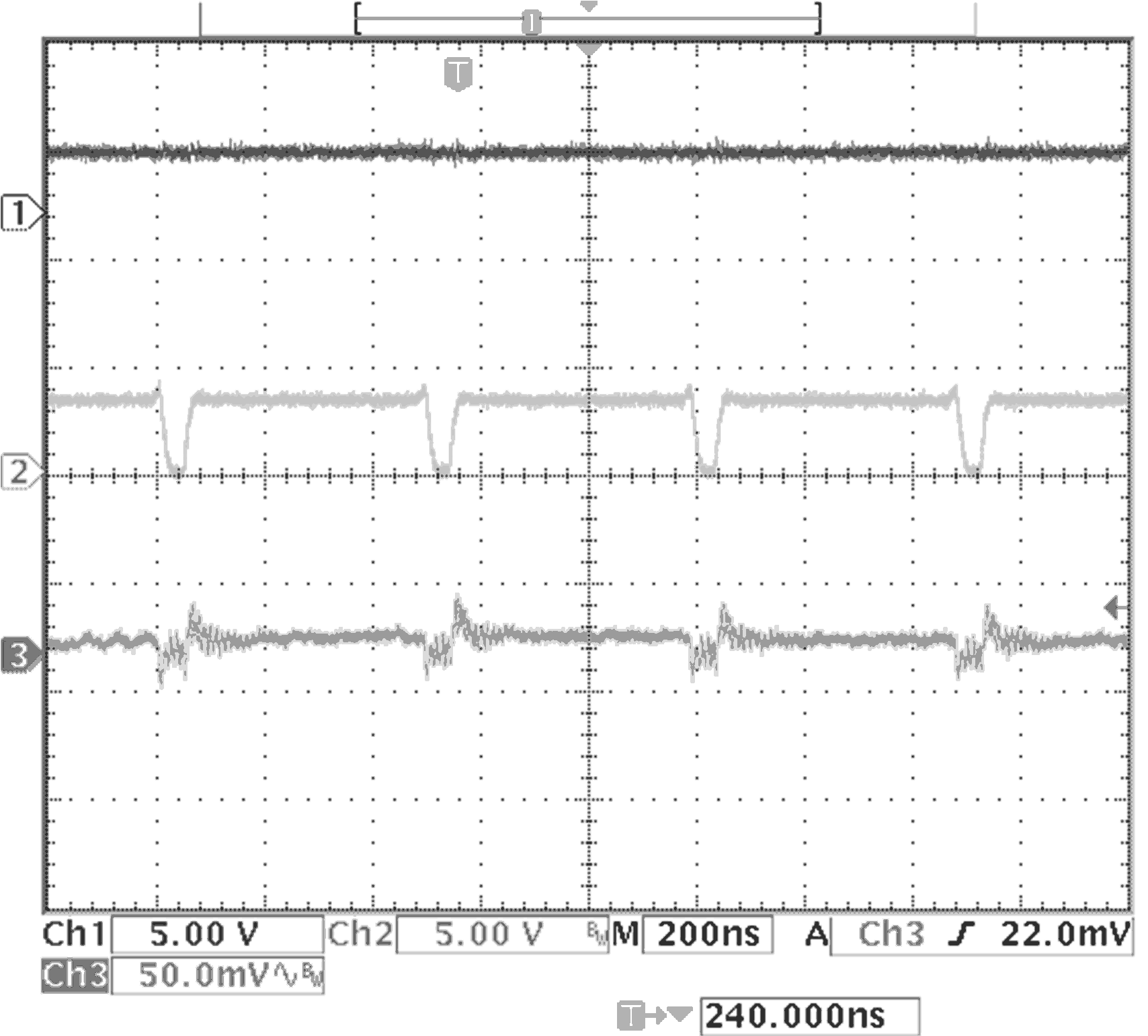
| VIN = 3.2 V | VOUT = 3.3 V | ILOAD = 250 mA |
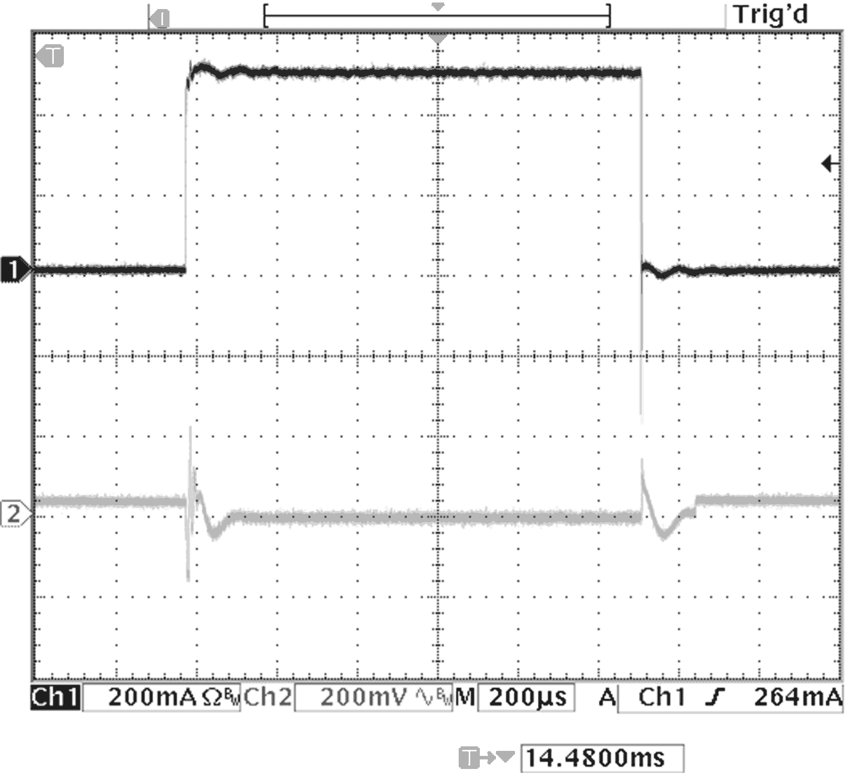
| VIN = 3.6 V | VOUT = 3.3 V | ILOAD = 0 to 500 mA |
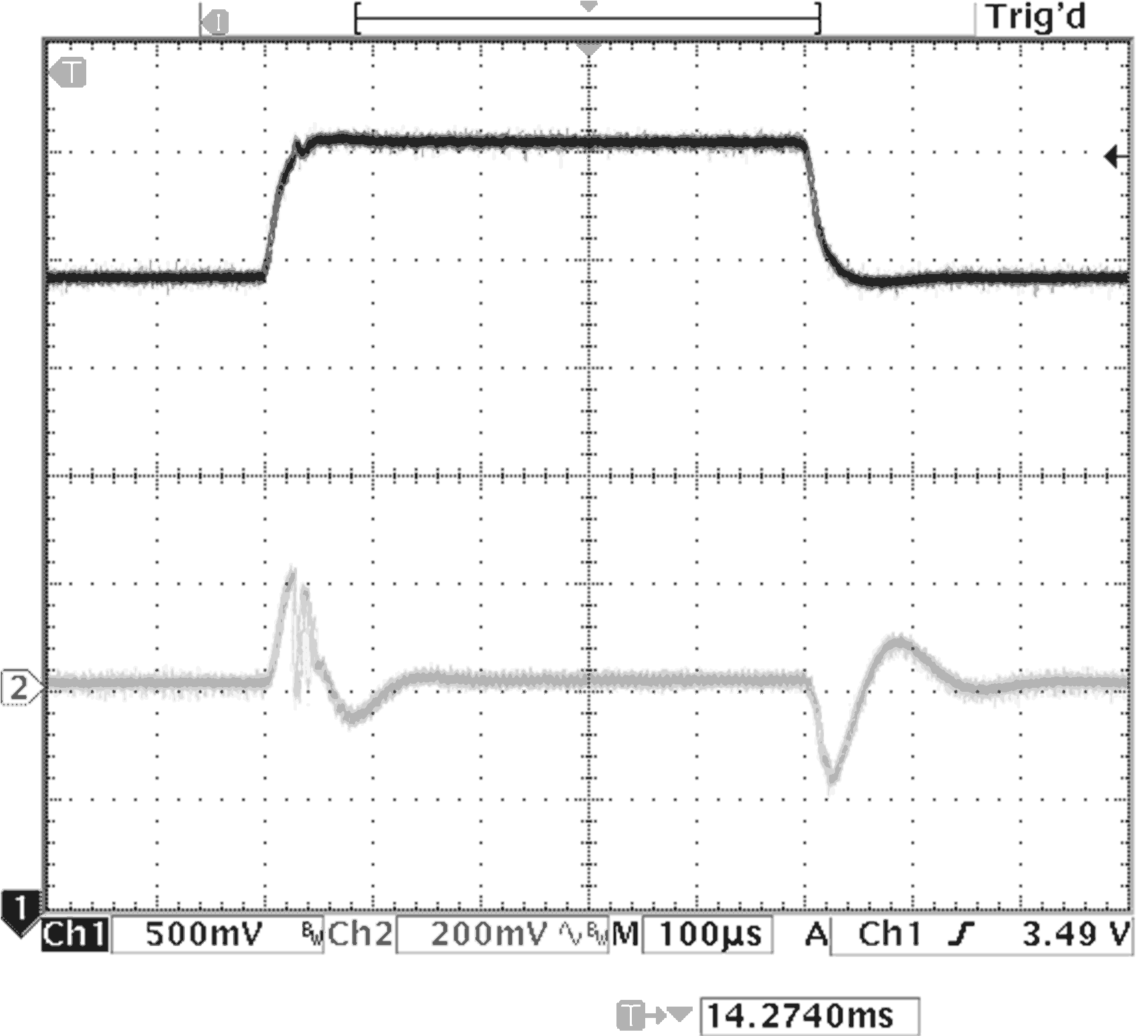
| VIN = 3 V to 3.6 V | VOUT = 3.3 V | ILOAD = 500 mA |