SNVS256E November 2003 – October 2024 LP3943
PRODUCTION DATA
- 1
- 1Features
- 2Applications
- 3Description
- 4Pin Configuration and Functions
- 5Specifications
- 6Detailed Description
- Application and Implementation
- 7Device and Documentation Support
- 8Revision History
- Mechanical, Packaging, and Orderable Information
Package Options
Mechanical Data (Package|Pins)
- RTW|24
Thermal pad, mechanical data (Package|Pins)
Orderable Information
6.5.4 Auto Increment
Auto increment is a special feature supported by the LP3943 to eliminate repeated chip and register addressing when data are to be written to or read from registers in sequential order. The auto increment bit is inside the register address byte, as shown in Figure 6-6. Auto increment is enabled when this bit is programmed to “1” and disabled when it is programmed to “0”.
Bits 5, 6 and 7 in the register address byte must always be zero.
 Figure 6-6 Register Address Byte
In the READ mode, when auto increment is enabled, I2C master could receive any number of bytes from LP3943 without selecting chip address and register address again. Every time the I2C master reads a register, the LP3943 increments the register address, and the next data register is read. When I2C master reaches the last register (09H), the register address rolls over to 00H.
In the WRITE mode, when auto increment is enabled, the LP3943 increments the register address every time I2C master writes to register. When the last register (09H register) is reached, the register address rolls over to 02H, not 00H, because the first two registers in LP3943 are read-only registers. It is possible to write to the first two registers independently, and the LP3943 device will acknowledge, but the data is ignored.
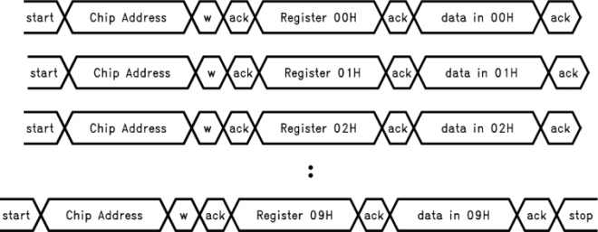
If auto increment is disabled, and the I2C master does not change register address, it continues to write data into the same register.
 Figure 6-7 Programming With Auto Increment Disabled (in WRITE Mode)
 Figure 6-8 Programming With Auto Increment Enabled (in WRITE Mode)