SLDS269A March   2022  – May 2022 LP5891

PRODUCTION DATA  

  1. Features
  2. Applications
  3. Description
  4. Revision History
  5. Pin Configuration and Functions
  6. Specifications
    1. 6.1 Absolute Maximum Ratings
    2. 6.2 ESD Ratings
    3. 6.3 Recommended Operating Conditions
    4. 6.4 Thermal Information
    5. 6.5 Electrical Characteristics
    6. 6.6 Timing Requirements
    7. 6.7 Switching Characteristics
    8. 6.8 Typical Characteristics
  7. Detailed Description
    1. 7.1 Overview
    2. 7.2 Functional Block Diagram
    3. 7.3 Feature Description
      1. 7.3.1 Independent and Stackable Mode
        1. 7.3.1.1 Independent Mode
        2. 7.3.1.2 Stackable Mode
      2. 7.3.2 Current Setting
        1. 7.3.2.1 Brightness Control (BC) Function
        2. 7.3.2.2 Color Brightness Control (CC) Function
        3. 7.3.2.3 Choosing BC/CC for a Different Application
      3. 7.3.3 Frequency Multiplier
      4. 7.3.4 Line Transitioning Sequence
      5. 7.3.5 Protections and Diagnostics
        1. 7.3.5.1 Thermal Shutdown Protection
        2. 7.3.5.2 IREF Resistor Short Protection
        3. 7.3.5.3 LED Open Load Detection and Removal
          1. 7.3.5.3.1 LED Open Detection
          2. 7.3.5.3.2 Read LED Open Information
          3. 7.3.5.3.3 LED Open Caterpillar Removal
        4. 7.3.5.4 LED Short and Weak Short Circuitry Detection and Removal
          1. 7.3.5.4.1 LED Short/Weak Short Detection
          2. 7.3.5.4.2 Read LED Short Information
          3. 7.3.5.4.3 LSD Caterpillar Removal
    4. 7.4 Device Functional Modes
    5. 7.5 Continuous Clock Series Interface
      1. 7.5.1 Data Validity
      2. 7.5.2 CCSI Frame Format
      3. 7.5.3 Write Command
        1. 7.5.3.1 Chip Index Write Command
        2. 7.5.3.2 VSYNC Write Command
        3. 7.5.3.3 MPSM Write Command
        4. 7.5.3.4 Standby Clear and Enable Command
        5. 7.5.3.5 Soft_Reset Command
        6. 7.5.3.6 Data Write Command
      4. 7.5.4 Read Command
    6. 7.6 PWM Grayscale Control
      1. 7.6.1 Grayscale Data Storage and Display
        1. 7.6.1.1 Memory Structure Overview
        2. 7.6.1.2 Details of Memory Bank
        3. 7.6.1.3 Write a Frame Data into Memory Bank
      2. 7.6.2 PWM Control for Display
    7. 7.7 Register Maps
      1. 7.7.1  FC0
      2. 7.7.2  FC1
      3. 7.7.3  FC2
      4. 7.7.4  FC3
      5. 7.7.5  FC4
      6. 7.7.6  FC14
      7. 7.7.7  FC15
      8. 7.7.8  FC16
      9. 7.7.9  FC17
      10. 7.7.10 FC18
      11. 7.7.11 FC19
      12. 7.7.12 FC20
      13. 7.7.13 FC21
  8. Application and Implementation
    1. 8.1 Application Information
    2. 8.2 Typical Application
      1. 8.2.1 Design Requirements
        1. 8.2.1.1 System Structure
        2. 8.2.1.2 SCLK Frequency
        3. 8.2.1.3 Internal GCLK Frequency
        4. 8.2.1.4 Line Switch Time
        5. 8.2.1.5 Blank Time Removal
        6. 8.2.1.6 BC and CC
      2. 8.2.2 Detailed Design Procedure
        1. 8.2.2.1 Chip Index Command
        2. 8.2.2.2 FC Registers Settings
        3. 8.2.2.3 Grayscale Data Write
        4. 8.2.2.4 VSYNC Command
        5. 8.2.2.5 LED Open/Short Read
      3. 8.2.3 Application Curves
  9. Power Supply Recommendations
  10. 10Layout
    1. 10.1 Layout Guidelines
    2. 10.2 Layout Example
  11. 11Device and Documentation Support
    1. 11.1 Documentation Support
      1. 11.1.1 Related Documentation
    2. 11.2 Receiving Notification of Documentation Updates
    3. 11.3 Support Resources
    4. 11.4 Trademarks
    5. 11.5 Electrostatic Discharge Caution
    6. 11.6 Glossary
  12. 12Mechanical, Packaging, and Orderable Information

Package Options

Mechanical Data (Package|Pins)
Thermal pad, mechanical data (Package|Pins)
Orderable Information
LED Open Caterpillar Removal

Figure 7-11 shows the caterpillar issue caused by open LED. Suppose the LED0-1 is an open LED. When line 0 is chosen and the OUT1 is turned on, the OUT1 voltage is forced to approach to VLED because of the broken path of the current source. However, the voltage of the un-chosen lines are below the Vclamp which is much lower than VLED, causing all LEDs which connect to the channel OUT1, light unwanted.
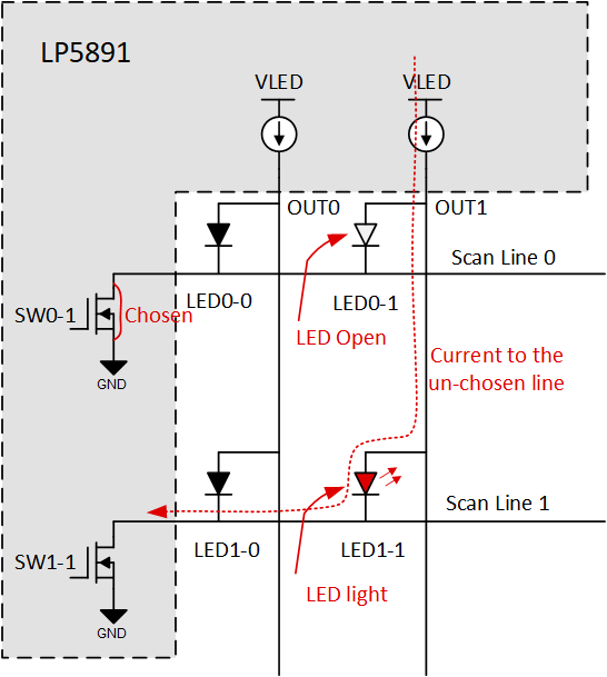
GUID-20211013-SS0I-FCRX-DCGZ-WX2T0Q9CBWPB-low.gif Figure 7-11 LED Open Caterpillar

The LP5891 implements circuits that can eliminate the caterpillar issue caused by open LEDs. The LED open caterpillar removal function is configured by LOD_RM_EN (see FC0 for more details). When LOD_RM_EN is set to 1b, the caterpillar removal function is enabled. The corresponding channel OUTn is turned off when scanning to line with open LED, The caterpillar issue is eliminated until device resets or LOD_RM_EN is set to 0b.

The internal caterpillar elimination circuit can handle a maximum of three lines that have open LEDs fault condition. If there are open LEDs located in three or fewer lines, the LP5891 is able to handle the open LEDs all in these lines. If there are open LEDs in more than three lines, the caterpillar issue is solved for the lines where the first three open LEDs were detected, but the open LEDs in the fourth and subsequent lines still cause the caterpillar issue.