SLDS269A March 2022 – May 2022 LP5891
PRODUCTION DATA
- 1 Features
- 2 Applications
- 3 Description
- 4 Revision History
- 5 Pin Configuration and Functions
- 6 Specifications
-
7 Detailed Description
- 7.1 Overview
- 7.2 Functional Block Diagram
- 7.3
Feature Description
- 7.3.1 Independent and Stackable Mode
- 7.3.2 Current Setting
- 7.3.3 Frequency Multiplier
- 7.3.4 Line Transitioning Sequence
- 7.3.5 Protections and Diagnostics
- 7.4 Device Functional Modes
- 7.5 Continuous Clock Series Interface
- 7.6 PWM Grayscale Control
- 7.7 Register Maps
- 8 Application and Implementation
- 9 Power Supply Recommendations
- 10Layout
- 11Device and Documentation Support
- 12Mechanical, Packaging, and Orderable Information
Package Options
Mechanical Data (Package|Pins)
Thermal pad, mechanical data (Package|Pins)
Orderable Information
7.3.1.2 Stackable Mode
While operating the LP5891 in stackable mode, as shown in below table.
| Mode | Matrix Size | Register Value | Scan Sequence |
|---|---|---|---|
| Mode1 | 16x32 | 000b | D1, D2 independent |
| Mode2 | 32x32 | 001b | D1->D2 |
| Mode3 | 48x48 | 010b | D1->D2->D3 |
| Mode4 | 48x48 | 011b | D1->D3->D2 |
| Mode5 | 48x64 | 100b | D1->D2->D3 |
| Mode6 | 48x64 | 101b | D1->D3->D2 |
| Mode7 | 64x64 | 110b | D1->D2->D3->D4 |
| Mode8 | 64x64 | 111b | D1->D4->D2->D3 |
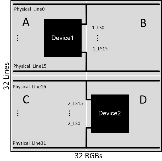
Figure 7-2 device 2 needs to be rotated 180o relative to device 1. This action allows the position of line switches to be near the center column of the LED matrix for better routing. For device 1, the lines connect sequentially (line switch 0 connected to scan line 1). However on device 2, it is connected in reverse order, with the 16th scan line is connected to line switch 15 and the 32nd scan line is connected to line switch 0.
Figure 7-2 shows the connection between two LP5891 devices in stackable mode driving 32 × 32 RGB LED pixels. The MOD_SIZE must be configured to 001b. Device 1 supplies 16 line switches for the first 16 scan line, and device 2 supplies 16 line switches for scan line 17-32. The data for matrix sections A and C are stored in device 1, while matrix sections B and D data are stored in device 2.
To make sure the scanning sequence is still from 1st line to 32nd line, the scan line switching order of the second device must be reversed, which can be configured by the SCAN_REV (see FC4 for more details).
 Figure 7-2 Mode2 Diagram
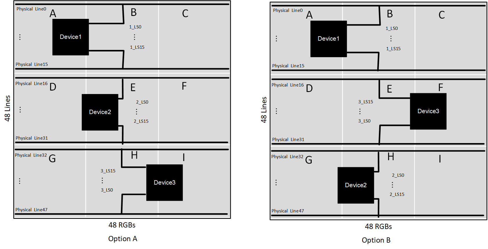
 Figure 7-3 Mode3 and Mode4 Diagram
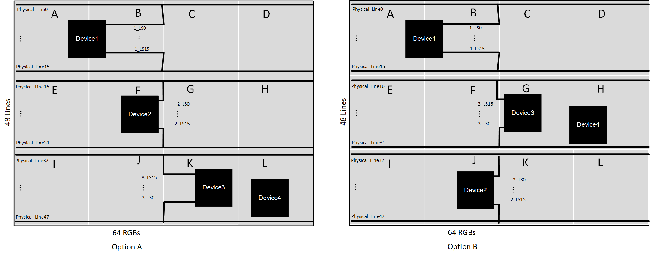
 Figure 7-4 Mode5 and Mode6 Diagram
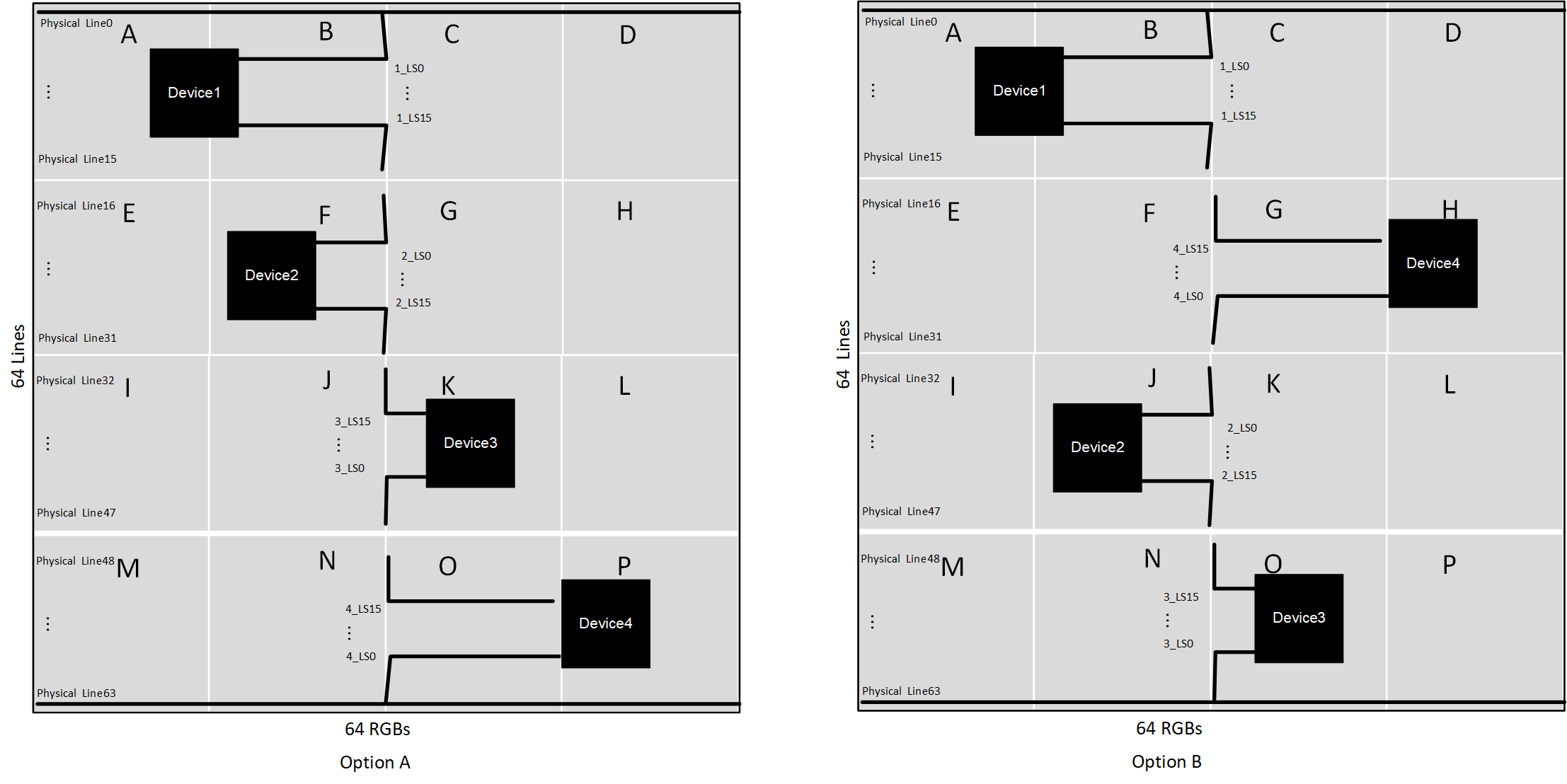
 Figure 7-5 Mode7 and Mode8 Diagram
When two or more LP5891 devices are used in stackable mode, if there are unused line switches, these unused line switches must be the last line switches of the first or the second device. For example, if there are only 30 scanning lines, and if,
SCAN_REV = '0'b, the unused line switches can be either of the below,
- 1_LS14, 1_LS15
- 2_LS14, 2_LS15
SCAN_REV = '1'b, the unused line switches can be either of below,
- 1_LS14, 1_LS15
- 2_LS1, 2_LS0
The unused line switches must be 2_LS14, 2_LS15 if SCAN_REV = '0'b, or 2_LS1, 2_LS0 if SCAN_REV = '1'b.