SLDS269A March   2022  – May 2022 LP5891

PRODUCTION DATA  

  1. Features
  2. Applications
  3. Description
  4. Revision History
  5. Pin Configuration and Functions
  6. Specifications
    1. 6.1 Absolute Maximum Ratings
    2. 6.2 ESD Ratings
    3. 6.3 Recommended Operating Conditions
    4. 6.4 Thermal Information
    5. 6.5 Electrical Characteristics
    6. 6.6 Timing Requirements
    7. 6.7 Switching Characteristics
    8. 6.8 Typical Characteristics
  7. Detailed Description
    1. 7.1 Overview
    2. 7.2 Functional Block Diagram
    3. 7.3 Feature Description
      1. 7.3.1 Independent and Stackable Mode
        1. 7.3.1.1 Independent Mode
        2. 7.3.1.2 Stackable Mode
      2. 7.3.2 Current Setting
        1. 7.3.2.1 Brightness Control (BC) Function
        2. 7.3.2.2 Color Brightness Control (CC) Function
        3. 7.3.2.3 Choosing BC/CC for a Different Application
      3. 7.3.3 Frequency Multiplier
      4. 7.3.4 Line Transitioning Sequence
      5. 7.3.5 Protections and Diagnostics
        1. 7.3.5.1 Thermal Shutdown Protection
        2. 7.3.5.2 IREF Resistor Short Protection
        3. 7.3.5.3 LED Open Load Detection and Removal
          1. 7.3.5.3.1 LED Open Detection
          2. 7.3.5.3.2 Read LED Open Information
          3. 7.3.5.3.3 LED Open Caterpillar Removal
        4. 7.3.5.4 LED Short and Weak Short Circuitry Detection and Removal
          1. 7.3.5.4.1 LED Short/Weak Short Detection
          2. 7.3.5.4.2 Read LED Short Information
          3. 7.3.5.4.3 LSD Caterpillar Removal
    4. 7.4 Device Functional Modes
    5. 7.5 Continuous Clock Series Interface
      1. 7.5.1 Data Validity
      2. 7.5.2 CCSI Frame Format
      3. 7.5.3 Write Command
        1. 7.5.3.1 Chip Index Write Command
        2. 7.5.3.2 VSYNC Write Command
        3. 7.5.3.3 MPSM Write Command
        4. 7.5.3.4 Standby Clear and Enable Command
        5. 7.5.3.5 Soft_Reset Command
        6. 7.5.3.6 Data Write Command
      4. 7.5.4 Read Command
    6. 7.6 PWM Grayscale Control
      1. 7.6.1 Grayscale Data Storage and Display
        1. 7.6.1.1 Memory Structure Overview
        2. 7.6.1.2 Details of Memory Bank
        3. 7.6.1.3 Write a Frame Data into Memory Bank
      2. 7.6.2 PWM Control for Display
    7. 7.7 Register Maps
      1. 7.7.1  FC0
      2. 7.7.2  FC1
      3. 7.7.3  FC2
      4. 7.7.4  FC3
      5. 7.7.5  FC4
      6. 7.7.6  FC14
      7. 7.7.7  FC15
      8. 7.7.8  FC16
      9. 7.7.9  FC17
      10. 7.7.10 FC18
      11. 7.7.11 FC19
      12. 7.7.12 FC20
      13. 7.7.13 FC21
  8. Application and Implementation
    1. 8.1 Application Information
    2. 8.2 Typical Application
      1. 8.2.1 Design Requirements
        1. 8.2.1.1 System Structure
        2. 8.2.1.2 SCLK Frequency
        3. 8.2.1.3 Internal GCLK Frequency
        4. 8.2.1.4 Line Switch Time
        5. 8.2.1.5 Blank Time Removal
        6. 8.2.1.6 BC and CC
      2. 8.2.2 Detailed Design Procedure
        1. 8.2.2.1 Chip Index Command
        2. 8.2.2.2 FC Registers Settings
        3. 8.2.2.3 Grayscale Data Write
        4. 8.2.2.4 VSYNC Command
        5. 8.2.2.5 LED Open/Short Read
      3. 8.2.3 Application Curves
  9. Power Supply Recommendations
  10. 10Layout
    1. 10.1 Layout Guidelines
    2. 10.2 Layout Example
  11. 11Device and Documentation Support
    1. 11.1 Documentation Support
      1. 11.1.1 Related Documentation
    2. 11.2 Receiving Notification of Documentation Updates
    3. 11.3 Support Resources
    4. 11.4 Trademarks
    5. 11.5 Electrostatic Discharge Caution
    6. 11.6 Glossary
  12. 12Mechanical, Packaging, and Orderable Information

Package Options

Mechanical Data (Package|Pins)
Thermal pad, mechanical data (Package|Pins)
Orderable Information

MPSM Write Command

The MPSM command is used to control the intelligent power save mode of devices in the same matrix. The device detects all zero data in a stackable module and receives MPSM command in current frame, then when VSYNC command comes, all devices in the same matrix turn off. After the device detects that there is non-zero display data of the next frame, it gets out from intelligent power save mode until MSPM command comes in current frame.
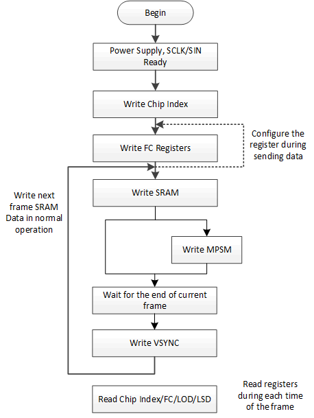
GUID-20211021-SS0I-T6SL-MS4F-LCFR7QXCKVR2-low.gif Figure 7-20 Design Procedure for MPSM Command