SNVSA91F September 2015 – April 2021 LP5910
PRODUCTION DATA
- 1 Features
- 2 Applications
- 3 Description
- 4 Revision History
- 5 Pin Configuration and Functions
- 6 Specifications
- 7 Detailed Description
- 8 Applications and Implementation
- 9 Power Supply Recommendations
- 10Layout
- 11Device and Documentation Support
Package Options
Mechanical Data (Package|Pins)
Thermal pad, mechanical data (Package|Pins)
- DRV|6
Orderable Information
3 Description
The LP5910 is a low-noise LDO that can supply up to 300 mA of output current. Designed to meet the requirements of RF and analog circuits, this device provides low noise, high PSRR, low quiescent current, and superior line transient and load transient response. Using new innovative design techniques the LP5910 offers class-leading noise performance without a noise bypass capacitor and with the option for remote output capacitor placement.
The device contains a reverse current protection circuit that prevents a reverse current flow through the LDO to the IN pin when the input voltage is lower than the output voltage.
When the Enable (EN) pin is low, and the output is in an OFF state, an automatic output discharge circuit discharges the output capacitance for fast turnoff.
With its low input and low output voltage range the LP5910 is well-suited as a post DC-DC regulator (post BUCK regulator) or for single- or dual-cell applications.
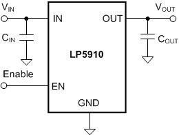
The device is designed to work with a 1-μF input and a 1-μF output ceramic capacitor. A separate noise bypass capacitor is not required.
This device is available with fixed output voltages from 0.8 V to 2.3 V in 25-mV steps. Contact Texas Instruments Sales for specific voltage option needs.
| PART NUMBER | PACKAGE | BODY SIZE |
|---|---|---|
| LP5910 | WSON (6) | 2.00 mm × 2.00 mm (NOM) |
| DSBGA (4) | 0.742 mm × 0.742 mm (MAX) |
 Simplified Schematic