SNVSC57 September 2022 LP5912-EP
PRODUCTION DATA
- 1 Features
- 2 Applications
- 3 Description
- 4 Revision History
- 5 Pin Configuration and Functions
- 6 Specifications
- 7 Detailed Description
- 8 Applications and Implementation
- 9 Device and Documentation Support
- 10Electrostatic Discharge Caution
- 11Glossary
- 12Mechanical, Packaging, and Orderable Information
Package Options
Mechanical Data (Package|Pins)
- DRV|6
Thermal pad, mechanical data (Package|Pins)
- DRV|6
Orderable Information
5 Pin Configuration and Functions
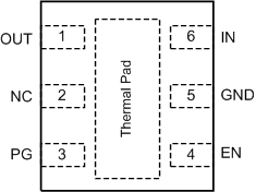
 Figure 5-1 DRV Package,6-Pin WSON With Thermal
Pad(Top
View)
Figure 5-1 DRV Package,6-Pin WSON With Thermal
Pad(Top
View)Table 5-1 Pin
Functions
| PIN | TYPE | DESCRIPTION | |
|---|---|---|---|
| NO. | NAME | ||
| 1 | OUT | O | Regulated output voltage. |
| 2 | NC | — | No internal connection. Leave open, or connect to ground. |
| 3 | PG | O | Power-good indicator. Requires an external pullup resistor. |
| 4 | EN | I | Enable input. Logic high = device is on, logic low = device is off, with an internal 3-MΩ pulldown resistor. |
| 5 | GND | G | Ground. |
| 6 | IN | I | Unregulated input voltage. |
| Thermal pad | — | Connect this pad to the copper area under the package to improve thermal performance. Use thermal vias to transfer heat to inner layers of the printed circuit board (PCB). Connect the thermal pad to ground, or leave floating. Do not connect the thermal pad to any potential other than ground. | |