SNVSC57 September   2022 LP5912-EP

PRODUCTION DATA  

  1. Features
  2. Applications
  3. Description
  4. Revision History
  5. Pin Configuration and Functions
  6. Specifications
    1. 6.1 Absolute Maximum Ratings
    2. 6.2 ESD Ratings
    3. 6.3 Recommended Operating Conditions
    4. 6.4 Thermal Information
    5. 6.5 Electrical Characteristics
    6. 6.6 Output and Input Capacitors
    7. 6.7 Typical Characteristics
  7. Detailed Description
    1. 7.1 Overview
    2. 7.2 Functional Block Diagram
    3. 7.3 Feature Description
      1. 7.3.1 Enable (EN)
      2. 7.3.2 Output Automatic Discharge (RAD)
      3. 7.3.3 Reverse Current Protection (IRO)
      4. 7.3.4 Internal Current Limit (ISC)
      5. 7.3.5 Thermal Overload Protection (TSD)
      6. 7.3.6 Power-Good Output (PG)
    4. 7.4 Device Functional Modes
      1. 7.4.1 Enable (EN)
      2. 7.4.2 Minimum Operating Input Voltage (VIN)
  8. Applications and Implementation
    1. 8.1 Application Information
    2. 8.2 Typical Application
      1. 8.2.1 Design Requirements
      2. 8.2.2 Detailed Design Procedure
        1. 8.2.2.1 External Capacitors
        2. 8.2.2.2 Input Capacitor
        3. 8.2.2.3 Output Capacitor
        4. 8.2.2.4 Capacitor Characteristics
        5. 8.2.2.5 Remote Capacitor Operation
        6. 8.2.2.6 Power Dissipation
        7. 8.2.2.7 Estimating Junction Temperature
      3. 8.2.3 Application Curves
    3. 8.3 Power Supply Recommendations
    4. 8.4 Layout
      1. 8.4.1 Layout Guidelines
      2. 8.4.2 Layout Example
  9. Device and Documentation Support
    1. 9.1 Documentation Support
      1. 9.1.1 Related Documentation
    2. 9.2 Receiving Notification of Documentation Updates
    3. 9.3 Support Resources
    4. 9.4 Trademarks
  10. 10Electrostatic Discharge Caution
  11. 11Glossary
  12. 12Mechanical, Packaging, and Orderable Information

Package Options

Mechanical Data (Package|Pins)
Thermal pad, mechanical data (Package|Pins)
Orderable Information

Description

The LP5912-EP is a low-noise, low-dropout regulator (LDO) that can supply up to 500 mA of output current. Designed to meet the requirements of RF and analog circuits, the LP5912-EP provides low noise, high PSRR, low quiescent current, and low line and load transient response. The LP5912-EP offers class-leading noise performance without a noise bypass capacitor and with the ability for remote output capacitance placement.

The device is designed to work with a 1-µF input and a 1-µF output ceramic capacitor (a separate noise bypass capacitor is not required).

This device is available with fixed output voltages from 0.8 V to 5.5 V in 25-mV steps. Contact the Texas Instruments Sales office for specific voltage option requirements.

Package Information(1)
PART NUMBER PACKAGE BODY SIZE (NOM)
LP5912-EP WSON (6) 2.00 mm × 2.00 mm
For all available packages, see the orderable addendum at the end of the data sheet.


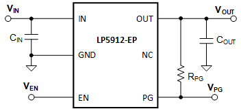
GUID-20220628-SS0I-ZHM6-BB30-HZCQH0VXPZ4H-low.gif Simplified Schematic