LP8754 Multi-Phase Six-Core Step-Down Converter
1 Features
- Six High-Efficiency Step-Down DC/DC Converter Cores:
- Max Output Current 10 A
- Cores Bundled to a 6-Phase Converter
- Load Current Reporting
- Programmable Overcurrent Protection (OCP)
- Auto PWM/PFM and Forced-PWM Operations and Automatic Low Power-Mode Setting
- Automatic Phase Adding/Shedding
- Remote Differential Feedback Voltage Sensing
- Output Voltage Ramp Control
- VOUT Range = 0.6 V to 1.67 V
- I2C-Compatible Interface which Supports Standard (100 kHz), Fast (400 kHz), and High-Speed (3.4 MHz) Modes
- Four Selectable I2C Addresses
- Interrupt Function with Programmable Masking
- Output Short-Circuit and Input Overvoltage Protection (OVP)
- Spread Spectrum and Phase Control for EMI Reduction
- Overtemperature Protection (OTP)
- Undervoltage Lock-out (UVLO)
2 Applications
- Smart Phones, eBooks and Tablets
- GSM, GPRS, EDGE, LTE, CDMA and WCDMA Handsets
- Gaming Devices
3 Description
The LP8754 is designed to meet the power management requirements of the latest applications processors in mobile phones and similar portable applications. The device contains six step-down DC/DC converter cores, which are bundled together in a 6-phase buck converter. The device is fully controlled by a Dynamic Voltage Scaling (DVS) interface or an I2C-compatible serial interface.
The automatic PWM/PFM operation together with the automatic phase adding/shedding maximizes efficiency over a wide output current range. The LP8754 supports remote differential voltage sensing to compensate IR drop between the regulator output and the point-of-load thus improving the accuracy of the output voltage.
The protection features include short-circuit protection, current limits, input OVP, UVLO, temperature warning, and shutdown functions. Several error flags are provided for status information of the IC. In addition, I2C read-back includes total load current and load current for each buck core: The LP8754 has the ability to sense current being delivered to the load without the addition of current sense resistors. During start-up, the device controls the output voltage slew rate to minimize overshoot and the inrush current.
Device Information(1)
| PART NUMBER | PACKAGE | BODY SIZE (MAX) |
|---|---|---|
| LP8754 | DSBGA (49) | 3.022 mm x 2.882 mm |
- For all available packages, see the orderable addendum at the end of the datasheet.
Efficiency vs. Load Current
4 Revision History
| DATE | REVISION | NOTES |
|---|---|---|
| August 2014 | Rev. A | Initial release to Web |
5 Pin Configuration and Functions
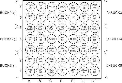
Pin Functions
| PIN | TYPE | DESCRIPTION | |
|---|---|---|---|
| NUMBER | NAME | ||
| A1, B1 | VINB2 | P | Input for Buck 2. The separate power pins VINBXX are not connected together internally - VINBXX pins must be connected together in the application and be locally bypassed. |
| A2, B2 | SWB2 | A | Buck 2 switch node |
| A3, B3, C3 | GNDB1/B2 | G | Power Ground for Buck 1 and Buck 2 |
| A4, B4 | SWB1 | A | Buck 1 switch node |
| A5, B5, C5 | VINB0/B1 | P | Input for Buck 0 and Buck 1. The separate power pins VINBXX are not connected together internally - VINBXX pins must be connected together in the application and be locally bypassed. |
| A6, B6 | SWB0 | A | Buck 0 switch node |
| A7, B7 | GNDB0 | G | Power Ground for Buck 0 |
| C1 | SDASYS | D/I/O | Serial interface data input and output for system access. Connect a pull-up resistor. |
| C2 | SCLSYS | D/I | Serial interface clock input for system access. Connect a pull-up resistor. |
| C4 | ADDR | D/I | Serial bus address selection. Connect to GND (addr = 60h), VIOSYS (addr = 61h), SDASYS (addr = 62h) or SCLSYS (addr = 63h). |
| C6 | NSLP | D/I | Full Power to Low Power state transition control signal (By default active LOW for Low-Power PFM mode) |
| C7 | VLDO | A | Internal supply voltage capacitor pin. A ceramic low ESR 1-µF capacitor should be connected from this pin to GNDA. The LDO voltage is generated internally, do NOT supply or load this pin externally. |
| D1 | FBB5 | A | Not used for six-phase converter. Connect to GND. |
| D2 | FBB3−/B4 | A | Not used for six-phase converter. Connect to GND. |
| D3 | FBB3+/B3 | A | Not used for six-phase converter. Connect to GND. |
| D4 | FBB2 | A | Not used for six-phase converter. Connect to GND. |
| D5 | FBB0−/B1 | A | Remote sensing (negative). Connect to the respective sense pin of the processor or to the negative power supply trace of the processor as close as possible to the processor. |
| D6 | FBB0+/B0 | A | Remote sensing (positive). Connect to the respective sense pin of the processor or to the positive power supply trace of the processor as close as possible to the processor. |
| D7 | GNDA | G | Ground |
| E1 | SDASR | D/I/O | Serial Interface data input and output for Dynamic Voltage Scaling (DVS). Connect a pull-up resistor / connect to GND if not used. |
| E2 | SCLSR | D/I | Serial Interface clock input for Dynamic Voltage Scaling (DVS). Connect a pull-up resistor / connect to GND if not used. |
| E3, F3, G3 | GNDB4/B5 | G | Power Ground for Buck 4 and Buck 5 |
| E4 | NRST | A | Voltage reference input for Dynamic Voltage Scaling (DVS) interface. Setting NRST input HIGH triggers start-up sequence. |
| E5, F5, G5 | VINB3/B4 | P | Input for Buck 3 and Buck 4.The separate power pins VINBXX are not connected together internally - VINBXX pins must be connected together in the application and be locally bypassed. |
| E6 | INT | D/O | Open-drain interrupt output. Active LOW. Connect a pull-up resistor to I/O supply. |
| E7 | VIOSYS | A | This pin shall be tied to the system I/O-voltage. Bias supply voltage for the device. Enables the I/O interface: All registers are accessible via serial bus interface when this pin is pulled high. An internal power-on reset (POR) occurs when VIOSYS is toggled low/high. The I2C host should allow at least 500 µs before sending data to the LP8754 after the rising edge of the VIOSYS line. |
| F1 | VDDA5V | P | Input for Analog blocks |
| F2, G2 | SWB5 | A | Buck 5 switch node |
| F4, G4 | SWB4 | A | Buck 4 switch node |
| F6, G6 | SWB3 | A | Buck 3 switch node |
| F7, G7 | GNDB3 | G | Power Ground for Buck 3 |
| G1 | VINB5 | P | Input for Buck 5. The separate power pins VINBXX are not connected together internally - VINBXX pins must be connected together in the application and be locally bypassed. |
| A: Analog Pin, D: Digital Pin, G: Ground Pin, P: Power Pin, I: Input Pin, O: Output Pin | |||
6 Specifications
6.1 Absolute Maximum Ratings (1)(2)
over operating free-air temperature range (unless otherwise noted)| MIN | MAX | UNIT | ||
|---|---|---|---|---|
| INPUT VOLTAGE | ||||
| Voltage on Power Connections (VIOSYS, VDDA5V, VINBXX) | −0.3 | 6 | V | |
| Voltage on Logic pins (Input or Output pins) (SCLSYS, SDASYS, NRST, NSLP, ADDR, INT, SCLSR, SDASR) | −0.3 | 6 | ||
| Buck switch nodes (SWBXX) | −0.3 | (VVINBXX + 0.2 V) with 6 V max | V | |
| VLDO, FBB0+/B0, FBB0−/B1, FBB2, FBB3+/B3, FBB3−/B4, FBB5 | −0.3 | 2 | V | |
| All other analog pins | −0.3 | 6 | ||
| TEMPERATURE | ||||
| Junction Temperature (TJ-MAX) | 150 | °C | ||
| Maximum Lead Temperature (Soldering, 10 s)(3) | 260 | |||
6.2 Handling Ratings
| MIN | MAX | UNIT | |||
|---|---|---|---|---|---|
| Tstg | Storage temperature range | −65 | 150 | °C | |
| V(ESD) (All pins)(1) | Electrostatic discharge | Human body model (HBM), per ANSI/ESDA/JEDEC JS-001, all pins(2) | –1000 | 1000 | V |
| Charged device model (CDM), per JEDEC specification JESD22-C101, all pins(3) | –250 | 250 | |||
6.3 Recommended Operating Conditions (2)
over operating free-air temperature range (unless otherwise noted)| MIN | MAX | UNIT | ||
|---|---|---|---|---|
| INPUT VOLTAGE | ||||
| Voltage on power connections (VDDA5V, VINBXX) | 2.5 | 5 | V | |
| Voltage on VIOSYS | 1.8 | smaller of 3.3 V or VVINBXX | V | |
| SCLSYS, SDASYS, ADDR | 0 | VVIOSYS | V | |
| SCLSR, SDASR, NSLP, INT | 0 | VNRST | V | |
| NRST | 0 | 1.8 | V | |
| TEMPERATURE | ||||
| Junction temperature (TJ) | −40 | 125 | °C | |
| Ambient temperature (TA) | −40 | 85 | ||
6.4 Thermal Information
| THERMAL METRIC(1) | LP8754 | UNIT | |
|---|---|---|---|
| YFQ | |||
| 49 PINS | |||
| RθJA | Junction-to-ambient thermal resistance | 49.2 | °C/W |
| RθJCtop | Junction-to-case (top) thermal resistance | 0.2 | |
| RθJB | Junction-to-board thermal resistance | 6.6 | |
| ψJT | Junction-to-top characterization parameter | 2.9 | |
| ψJB | Junction-to-board characterization parameter | 6.5 | |
| RθJCbot | Junction-to-case (bottom) thermal resistance | n/a | |
6.5 General Electrical Characteristics(1)(2)
Limits apply over the full ambient temperature range -40°C ≤ TA ≤ 85°C, VVDDA5V = VVINBXX = 3.7 V, VVIOSYS = VNRST = 1.8 V, VOUT = 1.1 V, (unless otherwise noted).| SYMBOL | PARAMETER | TEST CONDITIONS | MIN | TYP | MAX | UNIT |
|---|---|---|---|---|---|---|
| CURRENTS | ||||||
| ISHDN | Shutdown supply current. Total current into power connections VDDA5V and VINBXX | VVIOSYS = 0 V, VNRST = 0 V | 0.1 | 2 | µA | |
| ISTBY | Standby mode supply current. Total current into power connections VDDA5V and VINBXX | VVIOSYS = 1.8 V, VNRST = 0 V | 50 | |||
| IActive | Active mode current consumption. Total current into power connections VDDA5V and VINBXX | Low-power PFM Mode, no load, one core active | 130 | µA | ||
| PFM Mode, no load, one core active | 400 | µA | ||||
| Forced PWM Mode, no load, one core active | 14.5 | mA | ||||
| LOGIC AND CONTROL INPUTS SCLSYS, SDASYS, ADDR | ||||||
| VIL | Input low level | VVIOSYS = 1.8 V to 3.3 V | 0.3 x VVIOSYS | V | ||
| VIH | Input high level | VVIOSYS = 1.8 V to 3.3 V | 0.7 x VVIOSYS | |||
| Vhys | Hysteresis of Schmitt trigger inputs (SCLSYS, SDASYS) | 0.1 x VVIOSYS | ||||
| Ci | Capacitance of pins | See (3) | 4 | pF | ||
| LOGIC AND CONTROL INPUTS SCLSR, SDASR, NSLP, NRST | ||||||
| VIL | Input low level | VNRST = 1.8 V | 0.3 x VNRST | V | ||
| VIH | Input high level | VNRST = 1.8 V | 0.7 x VNRST | |||
| Vhys | Hysteresis of Schmitt trigger inputs (SCLSR, SDASR) | 0.1 x VNRST | ||||
| Ci | Capacitance of SCLSR and SDASR pins | 4 | pF | |||
| RIN | Input resistance | NRST pulldown resistor to GND | 1200 | kΩ | ||
| VIL_NRST | Input low level NRST | 0.54 | V | |||
| VIH_NRST | Input high level NRST | 1.3 | ||||
| LOGIC AND CONTROL OUTPUTS | ||||||
| VOL | Output low level | Voltage on INT pin, ISINK = 3 mA, VNRST = VVIOSYS = 1.8 V |
0.4 | V | ||
| Voltage on SDASYS, SDASR, ISINK = 3 mA, VNRST = VVIOSYS = 1.8 V |
0.36 | |||||
| RP | External pull-up resistor for INT | To I/O Supply | 10 | kΩ | ||
| ALL LOGIC AND CONTROL INPUTS | ||||||
| ILEAK | Input current | All Logic Inputs over pin voltage range. Note that NRST pin does have an 1.2-MΩ internal pulldown resistor and current through this resistor is not included into ILEAK rating. TA = 25°C | −1 | 1 | µA | |
6.6 6-Phase Buck Electrical Characteristics
Limits apply over the full ambient temperature range -40°C ≤ TA ≤ 85°C, VVDDA5V = VVINBXX = 3.7 V, VVIOSYS = VNRST = 1.8 V, VOUT = 1.1 V, (unless otherwise noted).| SYMBOL | PARAMETER | TEST CONDITIONS | MIN | TYP | MAX | UNIT | |
|---|---|---|---|---|---|---|---|
| VFB | Differential feedback voltage (1)
VFB0+/B0 - VFB0-/B1 |
PWM Mode, VOUTSET = 0.6 V to 1.67 V, IOUT ≤ 10 A(2) |
min (VOUTSET - 2.5%, VOUTSET - 25 mV) | VOUTSET | max (VOUTSET + 2.5%, VOUTSET + 25 mV) | V | |
| PFM Mode, VOUTSET = 0.6 V to 1.67 V, IOUT ≤ 375 mA |
min (VOUTSET - 2.5%, VOUTSET - 25 mV) | VOUTSET | max (VOUTSET + 2.5%, VOUTSET + 25 mV) | ||||
| Low-Power PFM Mode, VOUTSET = 0.6 V to 1.67 V, IOUT ≤ 30 mA |
min (VOUTSET - 3%, VOUTSET - 30 mV) | VOUTSET | max (VOUTSET + 3%, VOUTSET + 30 mV) | ||||
| ILIMITP | High side switch current limit | 2.5 A register setting | 2050 | 2600 | 3300 | mA | |
| ILIMITN | Low side switch current limit | Reverse current | 650 | 900 | 1050 | ||
| VOUT | Output voltage | Range, Programmable by register setting | 0.6 | 1.0 | 1.67 | V | |
| Step | 10 | mV | |||||
| fSW | Switching frequency | 2.5 V ≤ VVINBXX ≤ 5 V | 2.7 | 3.0 | 3.4 | MHz | |
| RDSON_P | Pin-pin resistance for PFET | Test Current = 200 mA; Split FET | 120 | mΩ | |||
| Test Current = 200 mA; Full FET | 60 | ||||||
| RDSON_N | Pin-pin resistance for NFET | IOUT = –200 mA | 50 | ||||
| ILK_HS | High-side leakage current | VSW = 0 V, Per Buck Core | 2 | µA | |||
| ILK_LS | Low-side leakage current | VSW = 3.7 V = VVINBXX, Per Buck Core | 2 | ||||
| RPD | Pull-down resistor | Enabled via control register, Active only when converter disabled, Per Buck Core | 250 | Ω | |||
| RIN_FB | Differential feedback Input resistance (3) | TA = 25°C | 200 | 300 | 400 | kΩ | |
6.7 6-Phase Buck System Characteristics
Limits apply over the full ambient temperature range -40°C ≤ TA ≤ 85°C, VVDDA5V = VVINBXX = 3.7 V, VVIOSYS = VNRST = 1.8 V, VOUT = 1.1 V, (unless otherwise noted).| SYMBOL | PARAMETER | TEST CONDITIONS | MIN | TYP | MAX | UNIT | |
|---|---|---|---|---|---|---|---|
| KRAMP | Ramp timer | Programmable via control register (1) | mV/µs | ||||
| RAMP_B0[2:0] = 000 | 30 | ||||||
| RAMP_B0[2:0] = 001 | 15 | ||||||
| RAMP_B0[2:0] = 010 | 7.5 | ||||||
| RAMP_B0[2:0] = 011 | 3.8 | ||||||
| RAMP_B0[2:0] = 100 | 1.9 | ||||||
| RAMP_B0[2:0] = 101 | 0.94 | ||||||
| RAMP_B0[2:0] = 110 | 0.47 | ||||||
| RAMP_B0[2:0] = 111 | 0.23 | ||||||
| TSTART | Start-up time | Time from NRST-HIGH to start of switching | 25 | µs | |||
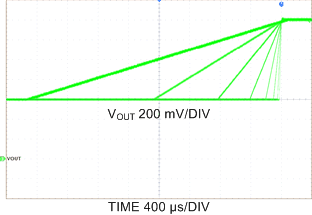
| TRAMP | VOUT rise time | Time to ramp from 5% to 95% of VOUT | 20 | µs | |||
| IPFM–PWM | PFM-to-PWM switch–over current threshold | Average output current, programmable via control register, VOUT = 1.1 V (2) | mA | ||||
| PFM_EXIT_B0[2:0] = 011 | 175 | ||||||
| PFM_EXIT_B0[2:0] = 100 | 225 | ||||||
| PFM_EXIT_B0[2:0] = 101 | 275 | ||||||
| PFM_EXIT_B0[2:0] = 110 | 325 | ||||||
| PFM_EXIT_B0[2:0] = 111 | 375 | ||||||
| IPWM–PFM | PWM-to-PFM switchover current threshold | Average output current, Programmable via control register, VOUT = 1.1 V (2) | mA | ||||
| PFM_ENTRY_B0[2:0] = 000 | 100 | ||||||
| PFM_ENTRY_B0[2:0] = 001 | 125 | ||||||
| PFM_ENTRY_B0[2:0] = 010 | 150 | ||||||
| PFM_ENTRY_B0[2:0] = 011 | 175 | ||||||
| PFM_ENTRY_B0[2:0] = 100 | 225 | ||||||
| IADD | Phase adding level | ADD_PH_B0[2:0] = 010 | 500 | mA | |||
| ADD_PH_B0[2:0] = 011 | 600 | ||||||
| ADD_PH_B0[2:0] = 100 | 700 | ||||||
| ADD_PH_B0[2:0] = 101 | 800 | ||||||
| ADD_PH_B0[2:0] = 110 | 900 | ||||||
| ADD_PH_B0[2:0] = 111 | 1000 | ||||||
| ISHED | Phase shedding level | SHED_PH_B0[2:0] = 000 | 300 | mA | |||
| SHED_PH_B0[2:0] = 001 | 400 | ||||||
| SHED_PH_B0[2:0] = 010 | 500 | ||||||
| SHED_PH_B0[2:0] = 011 | 600 | ||||||
| SHED_PH_B0[2:0] = 100 | 700 | ||||||
| SHED_PH_B0[2:0] = 101 | 800 | ||||||
| ΔVOUT | Line Regulation | 2.5 V ≤ VVINBXX ≤ 5 V ILOAD = 1 A, forced PWM |
0.05 | %/V | |||
| Load regulation in PWM mode of operation | 100 mA ≤ ILOAD ≤ 10 A, Differential sensing enabled | 0.2 | %/A | ||||
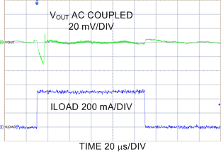
| Transient load step response | AUTO (no Low-Power PFM) mode, IOUT 0.5 mA → 500 mA → 0.5 mA, 100 ns load step | ±30 | mV | ||||
| PWM mode, IOUT 0.6 A → 2 A → 0.6 A, 400-ns load step | ±20 | mV | |||||
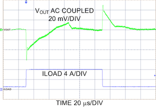
| PWM mode, IOUT 1 A → 8 A → 1 A, 400-ns load step | ±60 | mV | |||||
| Transient line response | VVINBXX stepping 3.3 V <—> 3.8 V, tr = tf = 10 µs, IOUT = 2000 mA DC |
±15 | mV | ||||
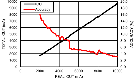
| IOUT | Output current | DC load each phase | 1670 | mA | |||
| Six phases combined(2) | 10000 | ||||||
| COUT | Output capacitance(4) | Effective capacitance during operation, VOUT = 0.6 V to 1.67 V, Min value over TA –40°C to 85°C | 30 | 50 | µF | ||
| CIN | Input capacitance on each input voltage rail (5)(4) | Effective capacitance during operation, 2.5 V ≤ VVINBXX ≤ 5 V, Min value over TA –40°C to 85°C | 2.5 | 10 | µF | ||
| L | Output inductance | Effective inductance during operation | 0.25 | 0.47 | 1 | µH | |
| IBALANCE | Current balancing accuracy | IOUT ≥ 1000 mA | < 10% | ||||
| VRIPPLE_PWM | Output voltage ripple PWM mode, One phase active(3) | COUT ESR = 10 mΩ PWM mode, IOUT = 200 mA Switching frequency = 3 MHz |
7 | mVPP | |||
| VRIPPLE_PFM | Output voltage ripple PFM mode(3) | COUT ESR = 10 mΩ PFM mode IOUT = 100 µA |
8 | mVPP | |||
| VRIPPLE_LP | Output Voltage Ripple Low-Power PFM mode(3) | COUT ESR = 10 mΩ Low-power PFM mode IOUT = 100 µA |
8 | mVPP | |||
6.8 Protection Features Characteristics
Limits apply over the full ambient temperature range -40°C ≤ TA ≤ 85°C, VVDDA5V = VVINBXX = 3.7 V, VVIOSYS = VNRST = 1.8 V, VOUT = 1.1 V, (unless otherwise noted).| SYMBOL | PARAMETER | TEST CONDITIONS | MIN | TYP | MAX | UNIT | |
|---|---|---|---|---|---|---|---|
| VOLTAGE MONITORING | |||||||
| VPG | Power good threshold voltage | Power good threshold for voltage decreasing, % of setting, VOUT = 1.1 V | 90% | ||||
| VOVP | Input overvoltage protection trigger point (1)(2) | VIN rising. Voltage monitored on VDDA5V pin | 5.15 | 5.30 | 5.45 | V | |
| VUVLO | Input undervoltage lockout (UVLO) turn-on threshold (1) | VIN falling. Voltage monitored on VDDA5V pin | 2.15 | 2.25 | 2.35 | ||
| VSCP | Output short-circuit fault threshold | Detected by sensing the voltage on converter output with respect to GND. | 400 | mV | |||
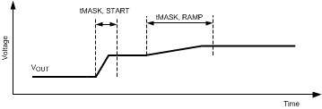
| tMASKSCP | SCP masking time | Triggered by converter start-up, specified by design | 400 | µs | |||
| tMASKPG | Power Good masking time | Triggered by converter start-up, specified by design | 400 | µs | |||
| Triggered by VSET transition, specified by design Slew Rate setting mV/µs |
|||||||
| 30 | 50 | µs | |||||
| 15 | 100 | ||||||
| 7.5 | 200 | ||||||
| 3.8 | 400 | ||||||
| 1.9 | 800 | ||||||
| 0.94 | 1600 | ||||||
| 0.47 | 3200 | ||||||
| 0.23 | 6400 | ||||||
| THERMAL SHUTDOWN AND MONITORING | |||||||
| TSHUT | Thermal shutdown (TSD) | Threshold, Temperature rising | 150 | °C | |||
| Hysteresis | 25 | ||||||
| TWARN | Thermal warning | Temperature rising, 1st warning, Interrupt only | 85 | ||||
| Hysteresis | 10 | ||||||
| Thermal warning prior to TSD | Temperature rising, 2nd warning, Interrupt and flag set | 120 | |||||
| Hysteresis | 10 | ||||||
6.9 I2C Serial Bus Timing Parameters
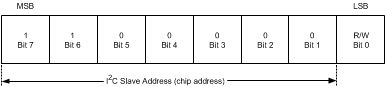
Serial bus address is selected by the ADDR pin. Connect the pin to GND (addr = 60h), VIOSYS (addr = 61h), SDASYS (addr = 62h), or SCLSYS (addr = 63h). Both of the serial buses share the same address; that is, if addr = 60h is selected for the System bus, the Dynamic Voltage Scaling bus will respond to the same address. Start conditions are used to secure the I2C slave address. During the I2C bus start condition, it is detected whether the ADDR is connected to SDASYS, SCLSYS, GND, or VIOSYS. The I2C host should allow at least 500 µs before sending data to the LP8754 after the rising edge of the VIOSYS line.These specifications are ensured by design. Limits apply over the full ambient temperature range -40°C ≤ TA ≤ 85°C, VVDDA5V = VVINBXX = 3.7 V, VVIOSYS = VNRST = 1.8 V, VOUT = 1.1 V, (unless otherwise noted).
| SYMBOL | PARAMETER (See Figure 1) | TEST CONDITIONS | MIN | TYP | MAX | UNIT | |
|---|---|---|---|---|---|---|---|
| DIGITAL TIMING SPECIFICATIONS (SCL, SDA)(1)(2)(4) | |||||||
| fCLK | Serial clock frequency | Standard mode | 100 | kHz | |||
| Fast mode | 400 | kHz | |||||
| High-speed mode, Cb = 100 pF (max) | 3.4 | MHz | |||||
| High-speed mode, Cb = 400 pF (max)(5) | 1.7 | MHz | |||||
| tLOW | SCL low time | Standard mode | 4.7 | µs | |||
| Fast mode | 1.3 | ||||||
| High-speed mode, Cb = 100 pF (max) | 160 | ns | |||||
| High-speed mode, Cb = 400 pF (max)(5) | 320 | ||||||
| tHIGH | SCL high time | Standard mode | 4.0 | µs | |||
| Fast mode | 0.6 | ||||||
| High-speed mode, Cb = 100 pF (max) | 60 | ns | |||||
| High-speed mode, Cb = 400 pF (max)(5) | 120 | ||||||
| tSU;DAT | Data setup time | Standard mode | 250 | ns | |||
| Fast mode | 100 | ||||||
| High-speed mode | 10 | ||||||
| tHD;DAT | Data hold time | Standard mode | 0 | 3.45 | µs | ||
| Fast mode | 0 | 0.9 | |||||
| High-speed mode, Cb = 100 pF (max) | 0 | 70 | ns | ||||
| High-speed mode, Cb = 400 pF (max)(5) | 0 | 150 | |||||
| tSU;STA | Set-up time for a repeated start condition | Standard mode | 4.7 | µs | |||
| Fast mode | 0.6 | ||||||
| High-speed mode | 160 | ns | |||||
| tHD;STA | Hold time for a start or a repeated start condition | Standard mode | 4.0 | µs | |||
| Fast mode | 0.6 | ||||||
| High-speed mode | 160 | ns | |||||
| tBUF | Bus free time between a stop and start condition | Standard mode | 4.7 | µs | |||
| Fast mode | 1.3 | ||||||
| tSU;STO | Set-up time for a stop condition | Standard mode | 4.0 | µs | |||
| Fast mode | 0.6 | ||||||
| High-speed mode | 160 | ns | |||||
| trDA | Rise time of SDA signal | Standard mode | 1000 | ns | |||
| Fast mode | 20 | 300 | ns | ||||
| High-speed mode, Cb = 100 pF (max) | 10 | 80 | ns | ||||
| High-speed mode, Cb = 400 pF (max)(5) | 20 | 160 | ns | ||||
| tfDA | Fall time of SDA signal | Standard mode | 300 | ns | |||
| Fast Mode | 6.5 | 300 | ns | ||||
| High-speed mode, Cb = 100 pF (max) | 10 | 80 | ns | ||||
| High-speed mode, Cb = 400 pF (max)(5) | 20 | 160 | ns | ||||
| trCL | Rise time of SCL signal | Standard mode | 1000 | ns | |||
| Fast mode | 20 | 300 | ns | ||||
| High-speed mode, Cb = 100 pF (max) | 10 | 40 | ns | ||||
| High-speed mode, Cb = 400 pF (max)(5) | 20 | 80 | ns | ||||
| trCL1 | Rise time of SCL signal after a repeated start condition and after anacknowledge bit | High-speed mode, Cb = 100 pF (max) | 10 | 80 | ns | ||
| High-speed mode, Cb = 400 pF (max)(5) | 20 | 160 | ns | ||||
| tfCL | Fall time of a SCL signal | Standard mode | 300 | ns | |||
| Fast mode | 6.5 | 300 | ns | ||||
| High-speed mode, Cb = 100 pF (max) | 10 | 40 | ns | ||||
| High-speed mode, Cb = 400 pF (max)(5) | 20 | 80 | ns | ||||
| Cb | Capacitive load for each bus line (SCL and SDA) | 400 | pF | ||||
| tSP | Pulse width of spike suppressed(3) | Fast mode | 50 | ns | |||
| High-speed mode | 10 | ||||||
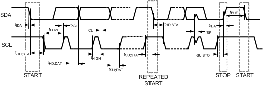 Figure 1. I2C Timing
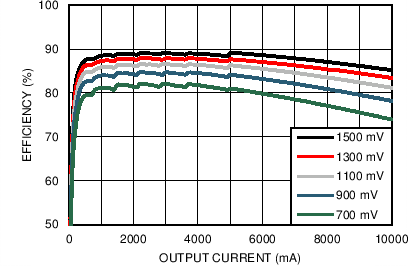
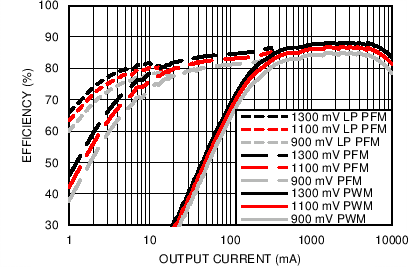
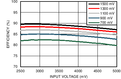
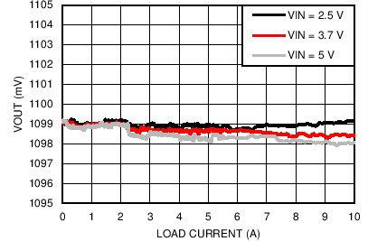
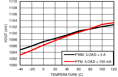
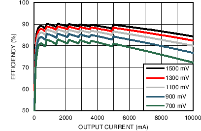
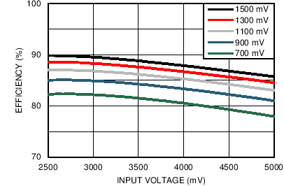
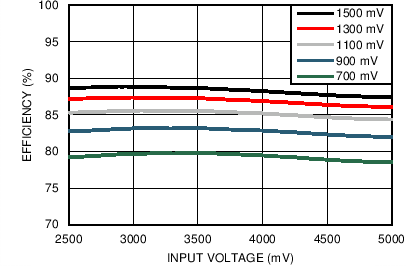
6.10 Typical Characteristics
Unless otherwise specified: VVDDA5V = VVINBXX = 3.7 V, VOUT = 1.1 V, TA = 25°C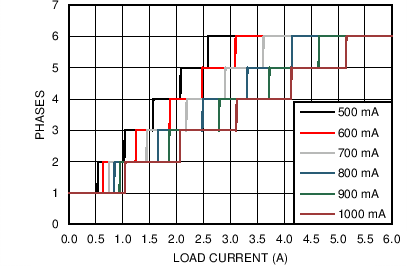
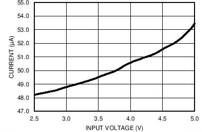
| VVIOSYS = 1.8 V | VNRST = 0 V |
| PFM Mode | No load | One core active |
| Low-Power Mode | No load | One core active |
| PWM Mode | No load | One core active |
7 Detailed Description
7.1 Overview
The LP8754 is a high-efficiency, high-performance power supply IC with six step-down DC-DC converter cores. It delivers 0.6 V to 1.67 V regulated voltage rail from either a single Li-Ion or three cell NiMH/NiCd batteries to portable devices such as cell phones and PDAs.
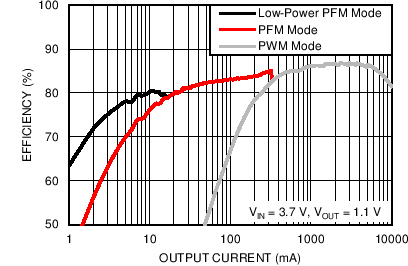
There are three modes of operation for the 6-phase converter, depending on the output current required: PWM (Pulse Width Modulation), PFM (Pulse-Frequency Modulation), and Low-Power PFM. Converter operates in PWM mode at high load currents of approximately 250 mA or higher, depending on register setting. Lighter output current loads will cause the converter to automatically switch into PFM or Low-Power PFM mode for reduced current consumption and a longer battery life. Forced PWM is also available for highest transient performance.
Under no-load conditions the device can be set to Standby or Shutdown. Shutdown mode turns off the device, offering the lowest current consumption (ISHDN = 0.1 µA typ.). Additional features include soft-start, undervoltage lockout, input overvoltage protection, current overload protection, thermal warning, and thermal shutdown.
The modes and features can be programmed via control registers. All the registers can be accessed with both I2C serial interfaces: System serial interface and Dynamic voltage scaling (DVS) interface. Using DVS interface for dynamic voltage scaling prevents latencies if System serial interface is busy. Using DVS interface is optional; System serial interface can also be used for dynamic voltage scaling.
7.1.1 Buck Information
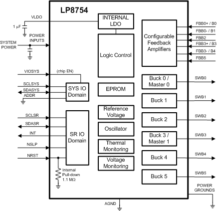
The LP8754 has six integrated high-efficiency buck converter cores. The cores are designed for flexibility; most of the functions are programmable, thus allowing optimization of the SMPS operation for each application. The cores are bundled together to establish a multi-phase converter This is shown in Figure 24.
Operating Modes:
- OFF: Output is isolated from the input voltage rail in this mode. Output has an optional pull-down resistor which can be enabled with BUCK0_CTRL.RDIS_B0 bit.
- PWM: Converter operates in buck configuration. Average switching frequency is constant.
- PFM: Converter switches only when output voltage decreases below programmed threshold. Inductor current is discontinuous.
- Low-Power PFM: This mode is similar to PFM mode, but used with lower load conditions. In this mode some of the internal blocks are turned off between the PFM pulses. Load transient response is compromised due to the wake-up time.
Features:
- DVS support
- Automatic mode control based on the loading
- Synchronous rectification
- Current mode loop with PI compensator
- Soft start
- Power good flag with maskable interrupt
- Overvoltage comparator
- Phase control and spread spectrum techniques for reducing EMI
- Average output current sensing (for PFM/PWM entry/exit, phase adding/shedding, and load current reporting)
- Current balancing between the phases of the converter
- Differential voltage sensing
- Dynamic phase adding/shedding, each output being phase shifted
Programmability (The following parameters can be programmed via registers):
- Output voltage
- Forced PWM operation
- Switch current limits for high side FET
- PWM/PFM mode entry and exit (based on average output current)
- Phase adding and shedding levels
- Output voltage slew rate
7.2 Functional Block Diagram
7.3 Features Descriptions
7.3.1 Multi-Phase DC/DC Converters
A multi-phase synchronous buck converter offers several advantages over a single power-stage converter. For application processor power delivery, lower ripple on the input and output currents and faster transient response to load steps are the most significant advantages. Also, since the load current is evenly shared among multiple channels, the heat generated is greatly reduced for each channel due to the fact that power loss is proportional to square of current. Physical size of the output inductor shrinks significantly for the similar reason.
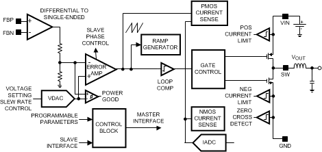 Figure 8. Detailed Block Diagram Showing One Buck Core
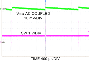
7.3.1.1 Multi-Phase Operation and Phase-Shedding
Under heavy load conditions, the switching phase of the bucks are interleaved. As a result, the 6-phase converter has higher effective switching frequency than the switching frequency of any one phase.
The parallel operation decreases the efficiency at low load conditions. In order to overcome this operational inefficiency, the LP8754 automatically changes the number of active phases to maximize the efficiency. This is called phase-shedding and the concept is illustrated in Figure 9.
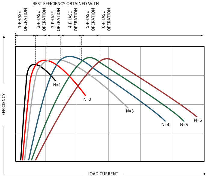 Figure 9. Multi-phase Buck Converter Efficiency vs Number of Phases; All Converters in PWM Mode
 7.3.1.2 Transitions Between Low-Power PFM, PFM, and PWM Modes
Normal PWM-mode operation with phase-shedding can optimize efficiency at mid-to-full load, but this is usually at the expense of light-load efficiency. The LP8754 converter operates in PWM mode at a load current of 100 to 375 mA or higher; this mode transition trip-point is set by register. Lighter load current causes the device to automatically switch into PFM mode for reduced current consumption. By combining PFM and PWM modes in the same regulator and providing automatic switching, high efficiency can be achieved over a wide output load current range.
Efficiency is further enhanced when the converter enters Low-Power PFM mode. The LP8754 includes Low-Power mode function for low-current consumption. In this mode most of the internal blocks are disabled between the inductor current ramp up and ramp down phases to reduce the operating current. However, as a result, the transient performance of the converter is compromised. The Low-Power mode can be enabled by control register setting. Also, the application processor or the PMIC may provide an HW signal (NSLP) to the LP8754 input to indicate when the processor has entered a low-power state. When the signal is asserted, the LP8754 Low-Power PFM function will be enabled, and the LP8754 will run with a reduced input current. The right timing of the NSLP signal from the system is important for best load-transient performance. The NSLP signal should be asserted only when load current is stable and below 30 mA. Before the load current increases above 30 mA, the NSLP signal should be de-asserted 100 µs (minimum) prior to a load step to prepare the converter for the higher load current.
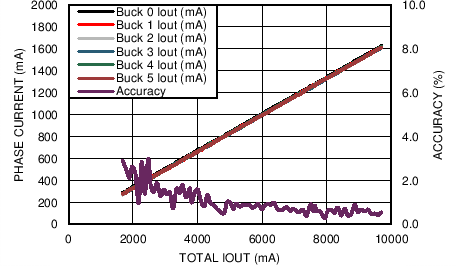
7.3.1.3 Buck Converter Load Current
The buck load current can be monitored via I2C registers. Current of different buck converter cores or the total load current of the master can be selected from register 0x21 (see SEL_I_LOAD). A write to this selection register starts a current measurement sequence. The measurement sequence is a minimum of 50 µs long. When a measurement sequence starts, the FLAGS_1.I_LOAD_READY bit in register 0x0E is set to '0'. After the measurement sequence is finished, the FLAGS_1.I_LOAD_READY bit is set to '1'. (Note that by default this bit is '0'.) The measurement result can be read from registers 0x22 (LOAD_CURR.BUCK_LOAD_CURR[7:0]) and 0x21 (SEL_I_LOAD.BUCK_LOAD_CURR[10:8]). The measurement result [10:0] LSB is 10 mA, and the maximum value of the measurement is 20 A. The LP8754 can be configured to give out an interrupt after the load current measurement sequence is finished. Load current measurement interrupt can be masked with INT_MASKS_2.MASK_I_LOAD_READY bit.
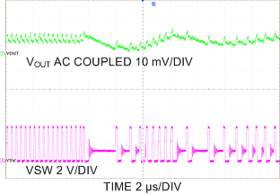
7.3.1.4 Spread Spectrum Mode
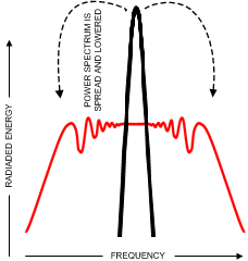
Systems with periodic switching signals may generate a large amount of switching noise in a set of narrowband frequencies (the switching frequency and its harmonics). The usual solution to reduce noise coupling is to add EMI-filters and shields to the boards. The LP8754's register-selectable spread spectrum mode minimizes the need for output filters, ferrite beads, or chokes. In spread spectrum mode, the switching frequency varies randomly around the center frequency, reducing the EMI emissions radiated by the converter, associated passive components, and PCB traces. See Figure 10.
7.3.2 Power-Up and Output Voltage Sequencing
The power-up sequence for the LP8754 is as follows:
- VVINBXX and VVDDA5V reach min recommended levels.
- VVIOSYS set high. Enables the system I/O interface. For power-on-reset (POR), the I2C host should allow at least 500 µs before sending data to the LP8754 after the rising edge of the VIOSYS line.
- VLDO voltage is raising. The LDO voltage is generated internally. The internal POR signal is activated.
- Internal POR deasserted, OTP read.
- Device enters standby mode.
- DC/DC enable, output voltage, voltage slew rate programmed over I2C as needed by the application.
- NRST set high. The DC/DC converter can be enabled and disabled by VSET_B0.EN_DIS_B0 bit or using the NRST signal.
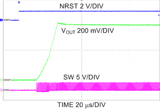
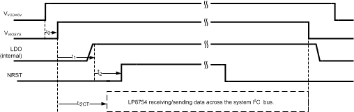 Figure 11. Timing Diagram for the Power-Up Sequence
Table 1. Power-Up Sequence
| SYMBOL | PARAMETER | CONDITION(1) | MIN | TYP | MAX | UNIT |
|---|---|---|---|---|---|---|
| t0 | VVDDA5V to VVIOSYS assertion | 0 | µs | |||
| t1 | LDOON Delay Time | CLDO = 1 µF | <100 | 150 | µs | |
| t2 | LDOON to NRST HIGH | 0 | µs | |||
| tI2CT | Device ready for I2C data transfer | 500 | µs |
7.3.3 Device Reset Scenarios
There are three reset methods implemented on the LP8754:
- Software reset
- Hardware reset
- Power-on reset (POR)
An SW-reset occurs when the RESET.SW_RESET bit is written first with 1, followed by 0 right after that. This event resets the control registers shown in Table 2 to the default values. The temperature, power good, and other faults are persistent over the SW reset to allow for the system to identify to cause of the failure.
An internal power-on reset (POR) occurs when the supply voltage (VVDDA5V) transitions above the POR threshold or VVIOSYS is toggled low/high. Each of the registers contain a factory-defined value upon POR, and this data remains there until any of the following occurs:
- Device sets a Flag bit, causing the Status register to be updated. The other registers remain untouched.
- A different data word is written to a writable register.
The internal registers will lose their contents if the supply voltage (VVDDA5V) goes below 1 V (typ.).
A hardware reset is accomplished by NRST low. This event resets the control registers shown in Table 2 to the default values.
Under OVP, UVLO, TSD, or VVIOSYS low (while NRST still high) conditions, a Fast Power-Down is launched.
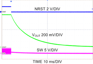
7.3.3.0.1 Normal Power-Down Sequence Follows This Event (Marked as '1')
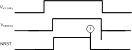 Figure 12. The External Power Control System De-asserts NRST
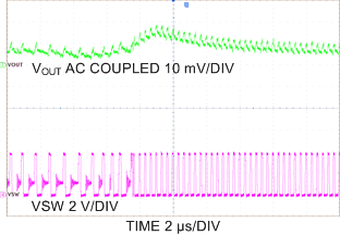
7.3.3.0.3 Inductor Current Dropping to Zero in ~2 µs (All Converters, All Phases)
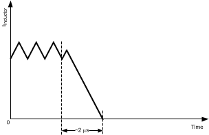 Figure 14. Fast Power-Down
 7.3.3.0.2 Fast Power-Down Follows This Event
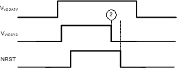 Figure 13. NRST Stays HIGH While VVIOSYS Transition from HIGH to LOW Happens (Marked as '2')
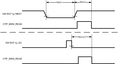 Figure 15. Reset Timings
| SYMBOL | PARAMETER | LIMIT |
|---|---|---|
| tRST1 | NRST active low pulse width | 1 µs min + value on DELAY_BUCK0 register. |
| tRST2 | NRST inactive or I2C reset event to MEMORY READ end | 25 µs max |
Table 2. Hardware Reset, Power-On Reset (POR) and Software Reset: Registers After Reset
| HEX ADDRESS | REGISTER | SOFTWARE RESET
I2C RESET |
HARDWARE RESET
NRST LOW(1) |
POWER-ON RESET
VVIOSYS LOW |
|---|---|---|---|---|
| 0x00 | VSET_B0 | All bits retained | All bits retained | All bits cleared |
| 0x06 | FPWM | All bits cleared | All bits cleared | All bits cleared |
| 0x07 to 0x0C | BUCK0_CTRL to BUCK5_CTRL | All bits cleared | All bits cleared | All bits cleared |
| 0x0D | FLAGS_0 | All bits retained | All bits retained | All bits cleared |
| 0x0E | FLAGS_1 | All bits retained | All bits retained | All bits cleared |
| 0x0F | INT_MASK0 | All bits cleared | All bits cleared | All bits cleared |
| 0x10 | GENERAL | All bits cleared | All bits cleared | All bits cleared |
| 0x11 | RESET | N/A | All bits cleared | All bits cleared |
| 0x12 | DELAY_BUCK0 | All bits cleared | All bits cleared | All bits cleared |
| 0x18 | CHIP_ID | Read Only | ||
| 0x19 | PFM_LEV_B0 | All bits cleared | All bits cleared | All bits cleared |
| 0x1F | PHASE_LEV_B0 | All bits cleared | All bits cleared | All bits cleared |
| 0x21 | SEL_I_LOAD | All bits retained | All bits retained | All bits cleared |
| 0x22 | LOAD_CURR | Read Only | ||
| 0x2E | INT_MASK_2 | All bits cleared | All bits cleared | All bits cleared |
7.3.4 Diagnosis and Protection Features
The LP8754 is capable of providing two levels of protection features: warnings for diagnosis and faults which are causing the converters to shut down. When the device detects warning or fault conditions, the LP8754 sets the flag bits indicating which fault or warning conditions have occurred; the INT pin will be pulled low. INT will be released again after a clear of flags is complete. The flag bits are persistent over reset to allow for the system to identify what was causing the interrupt and/or converter shutdown.
Also, the LP8754 has a soft-start circuit that limits in-rush current during start-up. The output voltage increase rate is 30 mV/µs (default) during soft-start.
Table 3. Summary of Exceptions and Interrupt Signals
| EVENT | REGISTER.BIT | INTERRUPT SIGNAL PRODUCED? | INT MASK AVAILABLE? |
|---|---|---|---|
| SCP triggered | FLAGS_1.SCP | Yes | Yes |
| Not PowerGood | FLAGS_0.nPG_B0 | Yes | Yes |
| TEMP status change | FLAGS_0.TEMP[1:0] | On any temperature change except for the case when TEMP[1:0] = 0b11 | Yes |
| Thermal warning | FLAGS_1.T_WARNING | Yes | Yes |
| Thermal shutdown | FLAGS_1.THSD | Yes | No |
| OVP triggered | FLAGS_1.OVP | Yes | Yes |
| Load current measurement ready | FLAGS_1.I_LOAD_READY | Yes | Yes |
| UVLO triggered | FLAGS_1.UVLO | Yes | Yes |
7.3.4.1 Warnings for Diagnosis (No Power Down)
7.3.4.1.1 Short-Circuit Protection (SCP)
A short-circuit protection feature allows the LP8754 to protect itself and external components during overload conditions. The output short-circuit fault threshold is 400 mV (typ.) .
7.3.4.1.2 Power Good Monitoring
When the converter's feedback-pin voltage falls lower than 90% (typ.) of the set voltage, the FLAGS_0.nPG_B0 flag is set. To prevent a false alarm, the power good circuit is masked during converter start-up and voltage transitions. The duration of the power good mask is set to 400 µs for converter start-up. For voltage ramps the masking time is extended by an internal logic circuit up to 6.4 ms. (See Protection Features Characteristics.)
7.3.4.1.3 Thermal Warnings
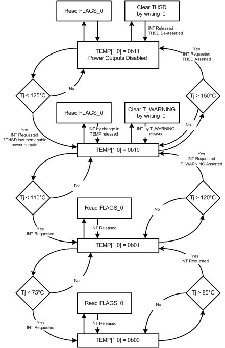
Prior to the thermal shutdown, thermal warnings are set. The first warning is set at 85°C (INT pin low), and the second at 120°C (INT pin pulled low and FLAGS_1.T_WARNING flag set). If the chip temperature crosses any of the thresholds of 85°C, 120°C, or 150°C (see FLAGS_0 register) the INT pin will be triggered. INT will be cleared upon read of FLAGS_0.TEMP[1:0] bits except if FLAGS_0.TEMP [1:0] = 0b11, which is a thermal fault event.
7.3.4.2 Faults (Fault State and Fast Power Down)
7.3.4.2.1 Undervoltage Lock-out (UVLO)
When the input voltage falls below VUVLO (typ. 2.25 V) at the VDDA5V pin, the LP8754 indicates a fault by activating the FLAGS_1.UVLO flag. The buck converter shut down without a power-down sequence (Fast Power-Down). The flag will remain active until the input voltage is raised above the UVLO threshold. If the flag is cleared while the fault persists, the flag is immediately re-asserted, and interrupt remains active.
7.3.4.2.2 Overvoltage Protection (OVP)
When an input voltage greater than VOVP (typ. 5.3 V) is detected at the VDDA5V pin, the LP8754 indicates a fault by activating the FLAGS_1.OVP flag. The buck converter is shut down immediately (Fast Power-Down). The flag will remain active until the input voltage is below the OVP threshold. If the flag is cleared while the fault persists, the flag is immediately re-asserted and interrupt remains active.
7.3.4.2.3 Thermal Shutdown (THSD)
The LP8754 has a thermal overload protection function that operates to protect itself from short-term misuse and overload conditions. When the junction temperature exceeds around 150°C, the device enters shutdown via fault-state. INT will be cleared upon write of the FLAGS_1.THSD flag even when thermal shutdown is active. This allows automatic recovery when temperature decreases below thermal shutdown level. See Figure 17 for LP8754 thermal diagnosis and protection features.
7.4 Device Functional Modes
-
SHUTDOWN:All switch, reference, control and bias circuitry of the LP8754 are turned off. The main battery supply voltage is high enough to start the buck power-up sequence but VVIOSYS and NRST are LOW.
-
STANDBY:Setting VVIOSYS HIGH enables standby-operation. All registers can be read or written by the system master via the system serial interface. Recovery from UVLO, TSD, or OVP event also leads to standby.
-
ACTIVE:Regulated DC/DC converters are on or can be enabled with full current capability. In this mode, all features and control registers are available via the system serial bus and via DVS interface.
-
LOW-POWER:At light loads (less than ~30 mA), and when the load does not require highest level of transient performance, the device enters automatically Low-Power mode. In this mode the part operates at low Iq. Conditions entering and exiting Low-Power mode are shown in Figure 18.
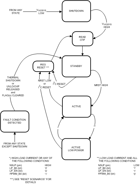 Figure 18. Device Operation Modes
7.5 Programming
7.5.1 I2C-Compatible Interface
The I2C-compatible synchronous serial interface provides access to the programmable functions and registers on the device. This protocol uses a two-wire interface for bidirectional communications between the IC's connected to the bus. The two interface lines are the Serial Data Line (SDA), and the Serial Clock Line (SCL). Every device on the bus is assigned a unique address and acts as either a Master or a Slave depending on whether it generates or receives the serial clock SCL. The SCL and SDA lines should each have a pull-up resistor placed somewhere on the line and remain HIGH even when the bus is idle. Note: CLK pin is not used for serial bus data transfer. There are two buses implemented: the System I2C bus and the DVS bus. In the following paragraphs, SCL refers to both SCLSYS and SCLSR, and SDA refers to SDASYS and SDASR. The LP8754 supports standard mode (100 kHz), fast mode (400 kHz) and high-speed mode (3.4 MHz).
7.5.1.1 Data Validity
The data on SDA line must be stable during the HIGH period of the clock signal (SCL). In other words, state of the data line can only be changed when clock signal is LOW.
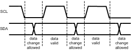 Figure 19. Data Validity Diagram
7.5.1.2 Start and Stop Conditions
The LP8754 is controlled via an I2C-compatible interface. START and STOP conditions classify the beginning and end of the I2C session. A START condition is defined as SDA transitions from HIGH to LOW while SCL is HIGH. A STOP condition is defined as SDA transition from LOW to HIGH while SCL is HIGH. The I2C master always generates the START and STOP conditions.
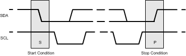 Figure 20. Start and Stop Sequences
The I2C bus is considered busy after a START condition and free after a STOP condition. During data transmission the I2C master can generate repeated START conditions. A START and a repeated START condition are equivalent function-wise. The data on SDA must be stable during the HIGH period of the clock signal (SCL). In other words, the state of SDA can only be changed when SCL is LOW. Figure 1 shows the SDA and SCL signal timing for the I2C-Compatible Bus. See the I2C Serial Bus Timing Parameters for timing values.
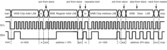
7.5.1.3 Transferring Data
Every byte put on the SDA line must be eight bits long, with the most significant bit (MSB) being transferred first. Each byte of data has to be followed by an acknowledge bit. The acknowledge related clock pulse is generated by the master. The master releases the SDA line (HIGH) during the acknowledge clock pulse. The LP8754 pulls down the SDA line during the 9th clock pulse, signifying an acknowledge. The LP8754 generates an acknowledge after each byte has been received.
There is one exception to the “acknowledge after every byte” rule. When the master is the receiver, it must indicate to the transmitter an end of data by not-acknowledging (“negative acknowledge”) the last byte clocked out of the slave. This “negative acknowledge” still includes the acknowledge clock pulse (generated by the master), but the SDA line is not pulled down.
After the START condition, the bus master sends a chip address. This address is seven bits long followed by an eighth bit which is a data direction bit (READ or WRITE). For the eighth bit, a “0” indicates a WRITE and a “1” indicates a READ. The second byte selects the register to which the data will be written. The third byte contains data to write to the selected register.
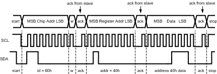 Figure 21. Write Cycle (w = write; SDA = '0'), id = device address = 60Hex for LP8754.
7.5.1.4 I2C-Compatible Chip Address
The device address for the LP8754 is 0x60 (ADDR pin tied to the GND). After the START condition, the I2C master sends the 7-bit address followed by an eighth bit, read or write (R/W). R/W = 0 indicates a WRITE and R/W = 1 indicates a READ. The second byte following the device address selects the register address to which the data will be written. The third byte contains the data for the selected register.
7.5.1.5 Auto-Increment Feature
The auto-increment feature allows writing several consecutive registers within one transmission. Every time an 8-bit word is sent to the LP8754, the internal address index counter will be incremented by one, and the next register will be written. Table 4 below shows writing sequence to two consecutive registers. Note: the auto-increment feature does not work for read.
Table 4. Auto-Increment Example
| Master Action | Start | Device Address = 60H | Write | Register Address | Data | Data | Stop | ||||
|---|---|---|---|---|---|---|---|---|---|---|---|
| LP8754 Action | ACK | ACK | ACK | ACK |
7.6 Register Maps
7.6.1 Register Descriptions
The LP8754 is controlled by a set of registers through the system serial interface port or through the Dynamic Voltage Scaling interface. Table 5 below lists device registers, their addresses and their abbreviations. A more detailed description is given in the sections VSET_B0 to INT_MASK_2.
Many registers contain bits, that are reserved for future use. When writing to a register, any reserved bits should not be changed.
Table 5.
| Addr | Register | Read / Write | D7 | D6 | D5 | D4 | D3 | D2 | D1 | D0 |
|---|---|---|---|---|---|---|---|---|---|---|
| 0x00 | VSET_B0 | R/W | EN_DIS_B0 | VSET_B0[6:0] | ||||||
| 0x06 | FPWM | R/W | Reserved | FPWM_B0 | ||||||
| 0x07 | BUCK0_CTRL | R/W | OC_LEV_B0[1:0] | LP_B0 | RDIS_B0 | Reserved | RAMP_B0[2:0] | |||
| 0x08 | BUCK1_CTRL | R/W | OC_LEV_B1[1:0] | Reserved | ||||||
| 0x09 | BUCK2_CTRL | R/W | OC_LEV_B2[1:0] | Reserved | ||||||
| 0x0A | BUCK3_CTRL | R/W | OC_LEV_B3[1:0] | Reserved | ||||||
| 0x0B | BUCK4_CTRL | R/W | OC_LEV_B4[1:0] | Reserved | ||||||
| 0x0C | BUCK5_CTRL | R/W | OC_LEV_B5[1:0] | Reserved | ||||||
| 0x0D | FLAGS_0 | R/W | Reserved | nPG_B0 | TEMP[1:0] | |||||
| 0x0E | FLAGS_1 | R/W | Reserved | I_LOAD_READY | UVLO | T_WARNING | THSD | OVP | SCP | |
| 0x0F | INT_MASK_0 | R/W | Reserved | MASK_nPG_B0 | MASK_OVP | MASK_SCP | ||||
| 0x10 | GENERAL | R/W | Reserved | EN_SS | Reserved | DIS_DIF_B0 | Reserved | SLP_POL | LP_EN | |
| 0x11 | RESET | R/W | Reserved | SW_RESET | ||||||
| 0x12 | DELAY_BUCK0 | R/W | DELAY_B0[7:0] | |||||||
| 0x18 | CHIP_ID | R | DEVICE | OTP_REV[4:0] | DIE_REV[1:0] | |||||
| 0x19 | PFM_LEV_B0 | R/W | Reserved | PFM_ENTRY_B0[2:0] | Reserved | PFM_EXIT_B0[2:0] | ||||
| 0x1F | PHASE_LEV_B0 | R/W | Reserved | ADD_PH_B0[2:0] | Reserved | SHED_PH_B0[2:0] | ||||
| 0x21 | SEL_I_LOAD | R/W | Reserved | BUCK_LOAD_CURR[10:8] | Reserved | LOAD_CURRENT_SOURCE[2:0] | ||||
| 0x22 | LOAD_CURR | R | BUCK_LOAD_CURR[7:0] | |||||||
| 0x2E | INT_MASK_2 | R/W | Reserved | MASK_ILOAD_READY | MASK_UVLO | MASK_TWARNING | MASK_TEMP | |||
7.6.2 VSET_B0
Address: 0x00
| D7 | D6 | D5 | D4 | D3 | D2 | D1 | D0 |
| EN_DIS_B0 | VSET_B0[6:0] | ||||||
| Bits | Field | Type | Default | Description |
|---|---|---|---|---|
| 7 | EN_DIS_B0 | R/W | 1 | DC/DC converter Buck0 Enable/Disable. The Enable of the master Buck0 controls the operation of the slave bucks. 0 = Converter disabled 1 = Converter enabled Note: When a disable request is received the converter is disabled immediately. |
| 6:0 | VSET_B0[6:0] | R/W | 011 1100 | Sets the output voltage. Defined by: VOUT = 0.5 V + 10 mV * VSET_B0 VOUT range = 0.6 V to 1.67 V NOTE: Do not use VSET_B0 values < 0001010 (10 dec) = 0.6 V. NOTE: Register settings starting from 1110110 up to 1111111 are clamped to 1.67 V. |
7.6.3 FPWM
Address: 0x06
| D7 | D6 | D5 | D4 | D3 | D2 | D1 | D0 |
| Reserved | FPWM_B0 | ||||||
| Bits | Field | Type | Default | Description |
|---|---|---|---|---|
| 7:1 | Reserved | R/W | 001 1111 | |
| 0 | FPWM_B0 | R/W | 1 | Forced PWM mode of operation, Buck regulator 0 (Master). The setting of the master controls the operation of the slave bucks. 0 = PWM, PFM or Low-Power PFM operation mode. 1 = This will force the master converter and the slaves to operate always in the PWM mode. |
7.6.4 BUCK0_CTRL
Address: 0x07
| D7 | D6 | D5 | D4 | D3 | D2 | D1 | D0 |
| OC_LEV_B0[1:0] | LP_B0 | RDIS_B0 | Reserved | RAMP_B0[2:0] | |||
| Bits | Field | Type | Default | Description |
|---|---|---|---|---|
| 7:6 | OC_LEV_B0[1:0] | R/W | 10 | Inductor positive current limit on Buck 0. Note that OC_LEV_B0...B5 should have the same value. 00 = 1.5 A 01 = 2.0 A 10 = 2.5 A 11 = 3.0 A |
| 5 | LP_B0 | R/W | 0 | Allows converter to enter into Low-Power PFM mode. 1 = Entering to Low-Power PFM mode is allowed. 0 = Entering to Low-Power PFM more is not allowed. |
| 4 | RDIS_B0 | R/W | 1 | Enables the output discharge resistors when the VOUT supply has been disabled. 1 = Enable pull-down 0 = Disable pull-down |
| 3 | Reserved | R/W | 0 | |
| 2:0 | RAMP_B0[2:0] | R/W | 001 | This set the output voltage change ramp as follows: 000 = 30 mV/µs 001 = 15 mV/µs 010 = 7.5 mV/µs 011 = 3.8 mV/µs 100 = 1.9 mV/µs 101 = 0.94 mV/µs 110 = 0.47 mV/µs 111 = 0.23 mV/µs |
7.6.5 BUCK1_CTRL
Address: 0x08
| D7 | D6 | D5 | D4 | D3 | D2 | D1 | D0 |
| OC_LEV_B1[1:0] | Reserved | ||||||
| Bits | Field | Type | Default | Description |
|---|---|---|---|---|
| 7:6 | OC_LEV_B1[1:0] | R/W | 10 | Inductor positive current limit on Buck 1. Note that OC_LEV_B0...B5 should have the same value. 00 = 1.5 A 01 = 2.0 A 10 = 2.5 A 11 = 3.0 A |
| 5:0 | Reserved | R/W | 01 0001 |
7.6.6 BUCK2_CTRL
Address: 0x09
| D7 | D6 | D5 | D4 | D3 | D2 | D1 | D0 |
| OC_LEV_B2[1:0] | Reserved | ||||||
| Bits | Field | Type | Default | Description |
|---|---|---|---|---|
| 7:6 | OC_LEV_B2[1:0] | R/W | 10 | Inductor positive current limit on Buck 2. Note that OC_LEV_B0...B5 should have the same value. 00 = 1.5 A 01 = 2.0 A 10 = 2.5 A 11 = 3.0 A |
| 5:0 | Reserved | R/W | 01 0001 |
7.6.7 BUCK3_CTRL
Address: 0x0A
| D7 | D6 | D5 | D4 | D3 | D2 | D1 | D0 |
| OC_LEV_B3[1:0] | Reserved | ||||||
| Bits | Field | Type | Default | Description |
|---|---|---|---|---|
| 7:6 | OC_LEV_B3[1:0] | R/W | 10 | Inductor positive current limit on Buck 3. Note that OC_LEV_B0...B5 should have the same value. 00 = 1.5 A 01 = 2.0 A 10 = 2.5 A 11 = 3.0 A |
| 5:0 | Reserved | R/W | 01 0001 |
7.6.8 BUCK4_CTRL
Address: 0x0B
| D7 | D6 | D5 | D4 | D3 | D2 | D1 | D0 |
| OC_LEV_B4[1:0] | Reserved | ||||||
| Bits | Field | Type | Default | Description |
|---|---|---|---|---|
| 7:6 | OC_LEV_B4[1:0] | R/W | 10 | Inductor positive current limit on Buck 4. Note that OC_LEV_B0...B5 should have the same value. 00 = 1.5 A 01 = 2.0 A 10 = 2.5 A 11 = 3.0 A |
| 5:0 | Reserved | R/W | 01 0001 |
7.6.9 BUCK5_CTRL
Address: 0x0C
| D7 | D6 | D5 | D4 | D3 | D2 | D1 | D0 |
| OC_LEV_B5[1:0] | Reserved | ||||||
| Bits | Field | Type | Default | Description |
|---|---|---|---|---|
| 7:6 | OC_LEV_B5[1:0] | R/W | 10 | Inductor positive current limit on Buck 5. Note that OC_LEV_B0...B5 should have the same value. 00 = 1.5 A 01 = 2.0 A 10 = 2.5 A 11 = 3.0 A |
| 5:0 | Reserved | R/W | 01 0001 |
7.6.10 FLAGS_0
Address: 0x0D
| D7 | D6 | D5 | D4 | D3 | D2 | D1 | D0 |
| Reserved | nPG_B0 | TEMP[1:0] | |||||
| Bits | Field | Type | Default | Description |
|---|---|---|---|---|
| 7:3 | Reserved | R/W | X XXXX | |
| 2 | nPG_B0 | R/W | 0 | Flag Bit (1)
Power good fault flag for VOUT rail 1 = Power fault detected 0 = Power good |
| 1:0 | TEMP[1:0] | R | 00 | indicates the die temperature as follows: 00: die temperature lower than 85ºC 01: 85ºC ≤ die temperature < 120ºC 10: 120ºC ≤ die temperature < 150ºC 11: die temperature 150ºC or higher |
7.6.11 FLAGS_1
Address: 0x0E
| D7 | D6 | D5 | D4 | D3 | D2 | D1 | D0 |
| Reserved | I_LOAD_READY | UVLO | T_WARNING | THSD | OVP | SCP | |
| Bits | Field | Type | Default | Description |
|---|---|---|---|---|
| 7:6 | Reserved | R/W | 00 | |
| 5 | I_LOAD_READY | R/W | 0 | Flag Bit(1)
1 = Buck load current measurement data ready 0 = Buck load current measurement data not ready |
| 4 | UVLO | R/W | 0 | Flag Bit (1)
1= Input undervoltage lockout (UVLO): Input voltage sagged below UVLO threshold. 0 = No UVLO |
| 3 | T_WARNING | R/W | 0 | Flag Bit (1)
1= Thermal warning: The IC temperature exceeds 120°C, in advance of the thermal shutdown protection. 0 = No thermal warning |
| 2 | THSD | R/W | 0 | Flag Bit (1)
1 = Thermal shutdown event detected 0 = No thermal shutdown |
| 1 | OVP | R/W | 0 | Flag Bit (1)
1= Indicates overvoltage protection (OVP) circuit activation. 0 = No OVP event. The OVP circuitry monitors VDDA5V power input. |
| 0 | SCP | R/W | 0 | Flag Bit (1)
1= Indicates short-circuit protection (SCP) circuit activation. The bit is activated when a short-circuit condition is detectedon output rail. 0 = No SCP event |
7.6.12 INT_MASK_0
Address: 0x0F
| D7 | D6 | D5 | D4 | D3 | D2 | D1 | D0 |
| Reserved | MASK_nPG_B0 | MASK_OVP | MASK_SCP | ||||
| Bits | Field | Type | Default | Description |
|---|---|---|---|---|
| 7:3 | Reserved | R/W | 1 1111 | |
| 2 | MASK_nPG_B0 | R/W | 0 | Interrupt mask for power good fault flag 1 = nPG_B0 does not set interrupt. 0 = nPG_B0 sets interrupt, when triggered. |
| 1 | MASK_OVP | R/W | 0 | Interrupt mask for Overvoltage Protection (OVP) fault flag 1 = OVP does not set interrupt. 0 = OVP sets interrupt, when triggered. |
| 0 | MASK_SCP | R/W | 0 | Interrupt mask for short-circuit protection SCP fault flag 1 = SCP does not set interrupt. 0 = SCP sets interrupt, when triggered. |
7.6.13 GENERAL
Address: 0x10
| D7 | D6 | D5 | D4 | D3 | D2 | D1 | D0 |
| Reserved | EN_SS | Reserved | DIS_DIF_B0 | Reserved | SLP_POL | LP_EN | |
| Bits | Field | Type | Default | Description |
|---|---|---|---|---|
| 7:6 | Reserved | R/W | 00 | |
| 5 | EN_SS | R/W | 0 | Spread Spectrum 1 = Spread Spectrum enabled 0 = Spread Spectrum disabled |
| 4 | Reserved | R/W | 0 | |
| 3 | DIS_DIF_B0 | R/W | 0 | Disable Differential-to-single-ended amplifier 1 = Differential amplifier disabled 0 = Differential amplifier enabled |
| 2 | Reserved | R/W | 0 | |
| 1 | SLP_POL | R/W | 0 | Sets the polarity of the NSLP pin 1 = NSLP is active high 0 = NSLP is active low |
| 0 | LP_EN | R/W | 1 | 1 = allows Low-Power PFM mode. In order to reduce power consumption under low load conditions, the unit will automatically switch off unused internal blocks. 0 = Low-Power mode not allowed |
7.6.14 RESET
Address: 0x11
| D7 | D6 | D5 | D4 | D3 | D2 | D1 | D0 |
| Reserved | SW_RESET | ||||||
| Bits | Field | Type | Default | Description |
|---|---|---|---|---|
| 7:1 | Reserved | R/W | 000 0000 | |
| 0 | SW_RESET | R/W | 0 | Writing this bit with '1' and '0', in this order, will reset the registers to the default values. If NRST is still kept HIGH, the converter output(s) will be regulated to the programmed register values. If a full POR reset is required VVIOSYS must be pulled low. The fault flags are persistent over SW-reset. |
7.6.15 DELAY_BUCK0
Address: 0x12
| D7 | D6 | D5 | D4 | D3 | D2 | D1 | D0 |
| DELAY_B0 | |||||||
| Bits | Field | Type | Default | Description |
|---|---|---|---|---|
| 7:0 | DELAY_B0 | R/W | 0000 0000 | Master delay Sets the delay time from when NRST is asserted to when the VOUT rail is enabled. Sets the delay time from when NRST is de-asserted to when the VOUT rail is disabled. DELAY = DELAY_B0 * 100 µs If DELAY_B0 = FFh, supply is never enabled. (1) |
7.6.16 CHIP_ID
Address: 0x18
| D7 | D6 | D5 | D4 | D3 | D2 | D1 | D0 |
| DEVICE | OTP_REV | DIE_REV | |||||
| Bits | Field | Type | Default | Description |
|---|---|---|---|---|
| 7 | DEVICE | R | 1 | DEVICE Contains Device ID |
| 6:2 | OTP_REV | R | 0 0001 | OTP_REV Contains OTP Version ID |
| 1:0 | DIE_REV | R | 00 | DIE_REV Contains Revision ID |
7.6.17 PFM_LEV_B0
Address: 0x19
| D7 | D6 | D5 | D4 | D3 | D2 | D1 | D0 |
| Reserved | PFM_ENTRY_B0[2:0] | Reserved | PFM_EXIT_B0[2:0] | ||||
| Bits | Field | Type | Default | Description |
|---|---|---|---|---|
| 7 | Reserved | R/W | 0 | |
| 6:4 | PFM_ENTRY_B0 | R/W | 011 | PFM_ENTRY_B0 (1)
Sets the target PFM entry level for Buck 0. The final PWM-to-PFM switchover current varies slightly and is dependant on the output voltage, input voltage and the inductor current level. 000 = 100 mA 001 = 125 mA 010 = 150 mA 011 = 175 mA 100 = 225 mA 101 = Reserved 110 = Reserved 111 = Reserved |
| 3 | Reserved | R/W | 0 | |
| 2:0 | PFM_EXIT_B0 | R/W | 110 | PFM_EXIT_B0 (1)
Sets the target PFM exit level for Buck 0. The final PFM-to-PWM switchover current varies slightly and is dependant on the output voltage, input voltage and the inductor current level. 000 = Reserved 001 = Reserved 010 = Reserved 011 = 175 mA 100 = 225 mA 101 = 275 mA 110 = 325 mA 111 = 375 mA |
7.6.18 PHASE_LEV_B0
Address: 0x1F
| D7 | D6 | D5 | D4 | D3 | D2 | D1 | D0 |
| Reserved | ADD_PH_B0[2:0] | Reserved | SHED_PH_B0[2:0] | ||||
| Bits | Field | Type | Default | Description |
|---|---|---|---|---|
| 7 | Reserved | R/W | 0 | |
| 6:4 | ADD_PH_B0 | R/W | 100 | ADD_PH_B0(1)
Sets the level on which a phase is added. 000 = Reserved 001 = Reserved 010 = 0.5 A * No. of Active Phases 011 = 0.6 A * No. of Active Phases 100 = 0.7 A * No. of Active Phases 101 = 0.8 A * No. of Active Phases 110 = 0.9 A * No. of Active Phases 111 = 1.0 A * No. of Active Phases |
| 3 | Reserved | R/W | 0 | |
| 2:0 | SHED_PH_B0 | R/W | 010 | SHED_PH_B0(1)
Sets the level of phase shedding. 000 = 0.3 A * No. of Active Phases 001 = 0.4 A * No. of Active Phases 010 = 0.5 A * No. of Active Phases 011 = 0.6 A * No. of Active Phases 100 = 0.7 A * No. of Active Phases 101 = 0.8 A * No. of Active Phases 110 = Reserved 111 = Reserved |
7.6.19 SEL_I_LOAD
Address: 0x21
| D7 | D6 | D5 | D4 | D3 | D2 | D1 | D0 |
| Reserved | BUCK_LOAD_CURR[10:8] | Reserved | LOAD_CURRENT_SOURCE[2:0] | ||||
| Bits | Field | Type | Default | Description |
|---|---|---|---|---|
| 7 | Reserved | R/W | 0 | |
| 6:4 | BUCK_LOAD_ CURR[10:8] |
R | 000 | BUCK_LOAD_CURR This register reports 3 MSB bits of the magnitude of the average load current of the selected Buck Converter. See LOAD_CURR register. |
| 3 | Reserved | R/W | 0 | |
| 2:0 | LOAD_CURRENT_ SOURCE[2:0] |
R/W | 000 | LOAD_CURRENT_SOURCE These bits are used for choosing the Buck Converter whose load current will be measured. 000 = Converter 0 load current will be measured. 001 = Converter 1 load current will be measured. 010 = Converter 2 load current will be measured. 011 = Converter 3 load current will be measured. 100 = Converter 4 load current will be measured. 101 = Converter 5 load current will be measured. 110 = Master total load current will be measured. 111 = Reserved |
7.6.20 LOAD_CURR
Address: 0x22
| D7 | D6 | D5 | D4 | D3 | D2 | D1 | D0 |
| BUCK_LOAD_CURR[7:0] | |||||||
| Bits | Field | Type | Default | Description |
|---|---|---|---|---|
| 7:0 | BUCK_LOAD_ CURR[7:0] |
R | 0000 0000 | BUCK_LOAD_CURR This register reports 8 LSB bits of the magnitude of the average load current of the selected Buck Converter. The value is reported with a resolution of 10 mA per LSB and 20A max current. Three MSB bits are reported by SEL_I_LOAD.BUCK_LOAD_CURR[10:8] bits, see SEL_I_LOAD. The current reported is an average over the last 5 milliseconds. The host system has read-only access to this register. This register is cleared to 0 on all resets. 000 0000 0000 Load current lower than 10 mA 000 0000 0001 10 mA ≤ Load current < 20 mA ... 111 1111 1110 20460 mA ≤ Load current < 20470 mA 111 1111 1111 Load current 20470 mA or higher. Note: Not production tested. Typical values for reference only. |
7.6.21 INT_MASK_2
Address: 0x2E
| D7 | D6 | D5 | D4 | D3 | D2 | D1 | D0 |
| Reserved | MASK_ILOAD_READY | MASK_UVLO | MASK_TWARNING | MASK_TEMP | |||
| Bits | Field | Type | Default | Description |
|---|---|---|---|---|
| 7:4 | Reserved | R/W | 0000 | |
| 3 | MASK_ILOAD_ READY |
R/W | 1 | Interrupt mask for load current measurement flag 1 = FLAGS_1.I_LOAD_READY does not set interrupt. 0 = FLAGS_1.I_LOAD_READY sets interrupt. |
| 2 | MASK_UVLO | R/W | 0 | Interrupt mask for undervoltage lock-out flag 1 = FLAGS_1.UVLO does not set interrupt. 0 = FLAGS_1.UVLO sets interrupt, when triggered. |
| 1 | MASK_ TWARNING |
R/W | 1 | Interrupt mask for thermal warning flag 1 = FLAGS_1.T_WARNING does not set interrupt. 0 = FLAGS_1.T_WARNING sets interrupt, when triggered. |
| 0 | MASK_TEMP | R/W | 1 | Interrupt mask for die temperature flag bits 1 = FLAGS_0.TEMP[1:0] value change does not set interrupt. 0 = FLAGS_0.TEMP[1:0] value change sets interrupt. |
8 Application and Implementation
8.1 Application Information
The LP8754 is a multi-phase step-down converter with 6 switcher cores bundled together.
8.2 Typical Application
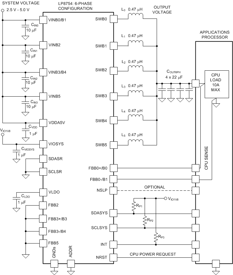 Figure 24. 6-Phase Configuration Schematic
8.2.1 Design Requirements
Table 6 shows requirements for 6-phase configuration.
Table 6. Design Parameters
| DESIGN PARAMETER | EXAMPLE VALUE |
|---|---|
| Input voltage range | 2.5 V to 5 V |
| Output voltage | 1.1 V |
| Converter operation mode | Forced PWM |
| Maximum load current | 10 A |
| Inductor current limit | 2.5 A |
8.2.2 Detailed Design Procedure
The performance of the LP8754 device depends greatly on the care taken in designing the Printed Circuit Board (PCB). The use of low inductance and low serial resistance ceramic capacitors is strongly recommended, while proper grounding is crucial. Attention should be given to decoupling the power supplies. Decoupling capacitors must be connected close to the IC and between the power and ground pins to support high peak currents being drawn from System Power Rail during turn-on of the switching MOSFETs. Keep input and output traces as short as possible, because trace inductance, resistance and capacitance can easily become the performance limiting items. The separate power pins VINBXX are not connected together internally. The VINBXX power connections shall be connected together outside the package using power plane construction.
8.2.2.1 Inductor Selection
The DC bias current characteristics of inductors must be considered. Different manufacturers follow different saturation current rating specifications, so attention must be given to details. (Please request DC bias curves from the manufacturer as part of the inductor selection process.) Minimum effective value of inductance to ensure good performance is 0.25 µH at 2.5 A (Default ILIMITP typ.) bias current over the inductor's operating temperature range. The inductor’s DC resistance should be less than 0.05 Ω for good efficiency at high-current condition. The inductor AC loss (resistance) also affects conversion efficiency. Higher Q factor at switching frequency usually gives better efficiency at light load to middle load. Table 7 below lists suggested inductors and suppliers. Shielded inductors radiate less noise and are preferable.
Table 7. Suggested Inductors
| ITEM | MODEL | VENDOR | DIMENSIONS LxWxH (mm) | D.C.R (mΩ) MAX |
|---|---|---|---|---|
| L0 to L5; Step-down converter inductor 0.47 µH | LQM21PNR47MGH DFE252012 R47 DFE201612C R47N |
Murata TOKO TOKO |
2.0 x 1.2 x 1.0 2.5 x 2 x 1.2 2.0 x 1.6 x 1.2 |
40 (typ) 39 50 |
8.2.2.2 Input Capacitor Selection
A ceramic input capacitor of 10 µF, 10 V is sufficient for most applications. Place the input capacitor as close as possible to the VINBXX pin and GND pin of the device. A larger value or higher voltage rating may be used to improve input voltage filtering. Use X7R or X5R types, do not use Y5V. DC bias characteristics of ceramic capacitors must be considered when selecting case sizes like 0402. Minimum effective input capacitance to ensure good performance is 2.5 µF at maximum input voltage DC bias including tolerances and over ambient temp range, assuming that there is at least 22 µF of additional capacitance common for all the power input pins on the system power rail.
The input filter capacitor supplies current to the PFET (high-side) switch in the first half of each cycle and reduces voltage ripple imposed on the input power source. A ceramic capacitor's low ESR provides the best noise filtering of the input voltage spikes due to this rapidly changing current. Select an input filter capacitor with sufficient ripple current rating.
For additional noise immunity, adding a high-frequency decoupling capacitor of 100 nF to 1 µF between VDDA5V pin and GND is recommended.
Table 8. Suggested Input/Output Capacitors (X5R Dielectric)
| MANUFACTURER | PART NUMBER | VALUE | CASE SIZE | VOLTAGE RATING |
|---|---|---|---|---|
| Murata | GRM188R60J106ME84 | 10 µF (20%) | 0603 | 6.3 V |
| TDK | C1608X5R1A106KT | 10 µF (10%) | 0603 | 10 V |
| Taiyo Yuden | LMK107BJ106MALTD | 10 µF (20%) | 0603 | 10 V |
| Samsung | CL10A226MP8NUNE | 22 µF (20%) | 0603 | 10 V |
| Samsung | CL03A105MQ3CSNH | 1 µF (20%) | 0201 | 6.3 V |
8.2.2.3 Output Capacitor Selection
Use ceramic capacitor, X7R or X5R types; do not use Y5V. DC bias voltage characteristics of ceramic capacitors must be considered. DC bias characteristics vary from manufacturer to manufacturer, and DC bias curves should be requested from them as part of the capacitor selection process. The output filter capacitor smooths out current flow from the inductor to the load, helps maintain a steady output voltage during transient load changes and reduces output voltage ripple. These capacitors must be selected with sufficient capacitance and sufficiently low ESR to perform these functions. Minimum effective output capacitance to ensure good performance in 6-phase configuration is 30 µF at the output voltage DC bias including tolerances and over ambient temp range.
The output voltage ripple is caused by the charging and discharging of the output capacitor and also due to its RESR. The RESR is frequency dependent (as well as temperature dependent); make sure the value used for selection process is at the switching frequency of the part. See suggested capacitors in Table 8.
A higher output capacitance improves the load step behavior and reduces the output voltage ripple as well as decreasing the PFM switching frequency. For most 6-phase applications 4 x 22 µF 0603 capacitors for COUT is suitable. Although the converter's loop compensation can be programmed to adapt to virtually several hundreds of microfarads COUT, an effective COUT less than 120 µF is preferred -- there is not necessarily any benefit to having a COUT higher than 120 µF. Note that the output capacitor may be the limiting factor in the output voltage ramp, especially for very large (> 100 µF) output capacitors. For large output capacitors, the output voltage might be slower than the programmed ramp rate at voltage transitions, because of the higher energy stored on the output capacitance. Also at start-up, the time required to charge the output capacitor to target value might be longer. At shutdown, if the output capacitor is discharged by the internal discharge resistor, more time is required to settle VOUT down as a consequence of the increased time constant.
8.2.2.4 LDO Capacitor Selection
A ceramic low ESR 1.0-μF capacitor should be connected between the VLDO and GNDA pins
8.2.2.5 VIOSYS Capacitor Selection
Adding a ceramic low ESR 1.0-μF capacitor between the VIOSYS pin and GND is recommended. If VVIOSYS signal is low noisy the capacitor is not required.
8.2.3 Application Performance Plots
Unless otherwise specified: VVDDA5V = VVINBXX = 3.7 V, VOUT = 1.1 V, TA = 25°C
| VIN = 3.7 V | Inductor: Murata LQM21PNR47MGH | |
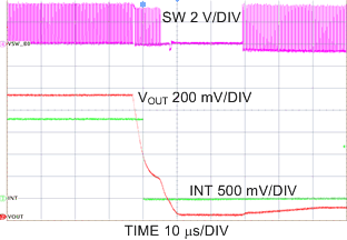
| VOUTSET = 900, 1100 and 1300 mV | ||
| Inductor: Murata LQM21PNR47MGH | ||
| IOUT = 3 A | Inductor: Murata LQM21PNR47MGH | |
| VOUTSET = 1.1 V |
| VOUTSET = 1.1 V |
| IOUT 1 A → 8 A → 1 A | tr = tf = 400 ns | |
| IOUT 0.5 mA → 0.5 A → 0.5 mA | ||
| tr = tf = 100 ns |
| IOUT = 100 µA |
| No Load |
| No Load | ||
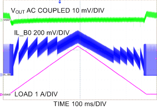
| IOUT 0 A → 5 A → 0 A | ||
| VIN = 2.7 V | Inductor: Murata LQM21PNR47MGH | |
| IOUT = 1 A | ||
| Inductor: Murata LQM21PNR47MGH | ||
| IOUT = 6 A | Inductor: Murata LQM21PNR47MGH | |
| VOUTSET = 1.1 V |
| ILOAD = 1.0 A | VOUTSET = 1.1 V |
| IOUT 0.6 A → 2 A → 0.6 A | tr = tf = 400 ns | |
| VIN 3.3 V → 3.8 V → 3.3 V | tr = tf = 10 µs | |
| IOUT = 2000 mA DC | ||
| IOUT = 200 mA |
| 3-A Load |