SNVS861A February 2014 – August 2014 LP8754
PRODUCTION DATA.
- 1 Features
- 2 Applications
- 3 Description
- 4 Revision History
- 5 Pin Configuration and Functions
-
6 Specifications
- 6.1 Absolute Maximum Ratings
- 6.2 Handling Ratings
- 6.3 Recommended Operating Conditions
- 6.4 Thermal Information
- 6.5 General Electrical Characteristics
- 6.6 6-Phase Buck Electrical Characteristics
- 6.7 6-Phase Buck System Characteristics
- 6.8 Protection Features Characteristics
- 6.9 I2C Serial Bus Timing Parameters
- 6.10 Typical Characteristics
-
7 Detailed Description
- 7.1 Overview
- 7.2 Functional Block Diagram
- 7.3 Features Descriptions
- 7.4 Device Functional Modes
- 7.5 Programming
- 7.6
Register Maps
- 7.6.1 Register Descriptions
- 7.6.2 VSET_B0
- 7.6.3 FPWM
- 7.6.4 BUCK0_CTRL
- 7.6.5 BUCK1_CTRL
- 7.6.6 BUCK2_CTRL
- 7.6.7 BUCK3_CTRL
- 7.6.8 BUCK4_CTRL
- 7.6.9 BUCK5_CTRL
- 7.6.10 FLAGS_0
- 7.6.11 FLAGS_1
- 7.6.12 INT_MASK_0
- 7.6.13 GENERAL
- 7.6.14 RESET
- 7.6.15 DELAY_BUCK0
- 7.6.16 CHIP_ID
- 7.6.17 PFM_LEV_B0
- 7.6.18 PHASE_LEV_B0
- 7.6.19 SEL_I_LOAD
- 7.6.20 LOAD_CURR
- 7.6.21 INT_MASK_2
- 8 Application and Implementation
- 9 Power Supply Recommendations
- 10Layout
- 11Device and Documentation Support
- 12Mechanical, Packaging, and Orderable Information
Package Options
Mechanical Data (Package|Pins)
- YFQ|49
Thermal pad, mechanical data (Package|Pins)
Orderable Information
10 Layout
10.1 Layout Guidelines
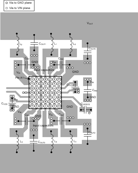
The high frequency and large switching currents of the LP8754 make the choice of layout important. Good power supply results will only occur when care is given to proper design and layout. Bad layout will affect noise pickup and generation and can cause a good design to perform with less-than-expected results. With a range of output currents from milliamps to 10 A, good power-supply layout is more challenging than for most general PCB design. The following steps should be used as a reference to ensure the device is stable and maintains proper voltage and current regulation across its intended operating voltage and current range:
- Place CIN as close as possible to the VINBXX pin and the GND pin. Route the VIN trace wide and thick to avoid IR drops. The trace between the input capacitor's positive node and LP8754’s VINBXX pin(s) as well as the trace between the input capacitor's negative node and power GND pin(s) must be kept as short as possible. The input capacitance provides a low-impedance voltage source for the switching converter. The parasitic inductance on these traces must be kept as tiny as possible for proper device operation.
- The output filter for each buck, consisting of COUT and L, converts the switching signal at SW to the noiseless output voltage. For optimal EMI behavior, it should be placed as close as possible to the device, keeping the switch node small. Route the traces between the LP8754's output capacitors and the load's input capacitors direct and wide to avoid losses due to the IR drop.
- Input for analog blocks (VDDA5V and GNDA) should be isolated from noisy signals. Connect VDDA5V directly to a quiet system voltage node and GNDA to a quiet ground point where no IR drop occurs. For additional noise immunity, adding a high-frequency decoupling capacitor of 100 nF to 1 µF is recommended. Place the decoupling capacitor as close to the VDDA5V pin as possible. VDDA5V trace is low current, so the trace width does not need to be optimized.
- If the processor load supports voltage remote sensing, connect the LP8754’s feedback pins FBBXX to the respective sense pins on the processor. The sense lines are susceptible to noise. They must be kept away from noisy signals such as GNDBXX, VIN, and SW, as well as high bandwidth signals such as the I2C. Avoid both capacitive as well as inductive coupling by keeping the sense lines short, direct, and close to each other. Run the lines in a quiet layer. Isolate them from noisy signals by a voltage or ground plane if possible. Running the signal as a differential pair is recommended.
- GNDBXX, VIN, and SW should be routed on thick layers. They must not surround inner signal layers which are not able to withstand interference from noisy GNDBXX, VIN, and SW. This can create noise coupling to inner signal layers.
Due to the small package of this converter and the overall small solution size, the thermal performance of the PCB layout is important. Many system-dependent issues such as thermal coupling, airflow, added heat sinks and convection surfaces, and the presence of other heat-generating components affect the power dissipation limits of a given component. Proper PCB layout, focusing on thermal performance, results in lower die temperatures. Wide power traces come with the ability to sink dissipated heat. This can be improved further on multi-layer PCB designs with vias to different planes. This results in reduced junction-to-ambient (RθJA) and junction-to-board (RθJB) thermal resistances, thereby reducing the device junction temperature, TJ. It's strongly recommended to perform a careful system-level 2D or full 3D dynamic thermal analysis at the beginning of the product design process, using a thermal modeling analysis software.
10.2 Layout Example
 Figure 54. LP8754 Board Layout