SNVS861A February 2014 – August 2014 LP8754
PRODUCTION DATA.
- 1 Features
- 2 Applications
- 3 Description
- 4 Revision History
- 5 Pin Configuration and Functions
-
6 Specifications
- 6.1 Absolute Maximum Ratings
- 6.2 Handling Ratings
- 6.3 Recommended Operating Conditions
- 6.4 Thermal Information
- 6.5 General Electrical Characteristics
- 6.6 6-Phase Buck Electrical Characteristics
- 6.7 6-Phase Buck System Characteristics
- 6.8 Protection Features Characteristics
- 6.9 I2C Serial Bus Timing Parameters
- 6.10 Typical Characteristics
-
7 Detailed Description
- 7.1 Overview
- 7.2 Functional Block Diagram
- 7.3 Features Descriptions
- 7.4 Device Functional Modes
- 7.5 Programming
- 7.6
Register Maps
- 7.6.1 Register Descriptions
- 7.6.2 VSET_B0
- 7.6.3 FPWM
- 7.6.4 BUCK0_CTRL
- 7.6.5 BUCK1_CTRL
- 7.6.6 BUCK2_CTRL
- 7.6.7 BUCK3_CTRL
- 7.6.8 BUCK4_CTRL
- 7.6.9 BUCK5_CTRL
- 7.6.10 FLAGS_0
- 7.6.11 FLAGS_1
- 7.6.12 INT_MASK_0
- 7.6.13 GENERAL
- 7.6.14 RESET
- 7.6.15 DELAY_BUCK0
- 7.6.16 CHIP_ID
- 7.6.17 PFM_LEV_B0
- 7.6.18 PHASE_LEV_B0
- 7.6.19 SEL_I_LOAD
- 7.6.20 LOAD_CURR
- 7.6.21 INT_MASK_2
- 8 Application and Implementation
- 9 Power Supply Recommendations
- 10Layout
- 11Device and Documentation Support
- 12Mechanical, Packaging, and Orderable Information
Package Options
Mechanical Data (Package|Pins)
- YFQ|49
Thermal pad, mechanical data (Package|Pins)
Orderable Information
6 Specifications
6.1 Absolute Maximum Ratings (1)(2)
over operating free-air temperature range (unless otherwise noted)| MIN | MAX | UNIT | ||
|---|---|---|---|---|
| INPUT VOLTAGE | ||||
| Voltage on Power Connections (VIOSYS, VDDA5V, VINBXX) | −0.3 | 6 | V | |
| Voltage on Logic pins (Input or Output pins) (SCLSYS, SDASYS, NRST, NSLP, ADDR, INT, SCLSR, SDASR) | −0.3 | 6 | ||
| Buck switch nodes (SWBXX) | −0.3 | (VVINBXX + 0.2 V) with 6 V max | V | |
| VLDO, FBB0+/B0, FBB0−/B1, FBB2, FBB3+/B3, FBB3−/B4, FBB5 | −0.3 | 2 | V | |
| All other analog pins | −0.3 | 6 | ||
| TEMPERATURE | ||||
| Junction Temperature (TJ-MAX) | 150 | °C | ||
| Maximum Lead Temperature (Soldering, 10 s)(3) | 260 | |||
(1) Stresses beyond those listed under absolute maximum ratings may cause permanent damage to the device. These are stress ratings only, and functional operation of the device at these or any other conditions beyond those indicated under recommended operating conditions is not implied. Exposure to absolute-maximum-rated conditions for extended periods may affect device reliability.
(2) All voltage values are with respect to network ground pin.
(3) For detailed soldering specifications and information, please refer to Application Note 1112: DSBGA Wafer-Level Chip-Scale Package (AN-1112).
6.2 Handling Ratings
| MIN | MAX | UNIT | |||
|---|---|---|---|---|---|
| Tstg | Storage temperature range | −65 | 150 | °C | |
| V(ESD) (All pins)(1) | Electrostatic discharge | Human body model (HBM), per ANSI/ESDA/JEDEC JS-001, all pins(2) | –1000 | 1000 | V |
| Charged device model (CDM), per JEDEC specification JESD22-C101, all pins(3) | –250 | 250 | |||
(1) Electrostatic discharge (ESD) to measure device sensitivity and immunity to damage caused by assembly line electrostatic discharges in to the device.
(2) JEDEC document JEP155 states that 500-V HBM allows safe manufacturing with a standard ESD control process.
(3) JEDEC document JEP157 states that 250-V CDM allows safe manufacturing with a standard ESD control process.
6.3 Recommended Operating Conditions (2)
over operating free-air temperature range (unless otherwise noted)| MIN | MAX | UNIT | ||
|---|---|---|---|---|
| INPUT VOLTAGE | ||||
| Voltage on power connections (VDDA5V, VINBXX) | 2.5 | 5 | V | |
| Voltage on VIOSYS | 1.8 | smaller of 3.3 V or VVINBXX | V | |
| SCLSYS, SDASYS, ADDR | 0 | VVIOSYS | V | |
| SCLSR, SDASR, NSLP, INT | 0 | VNRST | V | |
| NRST | 0 | 1.8 | V | |
| TEMPERATURE | ||||
| Junction temperature (TJ) | −40 | 125 | °C | |
| Ambient temperature (TA) | −40 | 85 | ||
6.4 Thermal Information
| THERMAL METRIC(1) | LP8754 | UNIT | |
|---|---|---|---|
| YFQ | |||
| 49 PINS | |||
| RθJA | Junction-to-ambient thermal resistance | 49.2 | °C/W |
| RθJCtop | Junction-to-case (top) thermal resistance | 0.2 | |
| RθJB | Junction-to-board thermal resistance | 6.6 | |
| ψJT | Junction-to-top characterization parameter | 2.9 | |
| ψJB | Junction-to-board characterization parameter | 6.5 | |
| RθJCbot | Junction-to-case (bottom) thermal resistance | n/a | |
(1) For more information about traditional and new thermal metrics, see the IC Package Thermal Metrics application report, SPRA953.
6.5 General Electrical Characteristics(1)(2)
Limits apply over the full ambient temperature range -40°C ≤ TA ≤ 85°C, VVDDA5V = VVINBXX = 3.7 V, VVIOSYS = VNRST = 1.8 V, VOUT = 1.1 V, (unless otherwise noted).| SYMBOL | PARAMETER | TEST CONDITIONS | MIN | TYP | MAX | UNIT |
|---|---|---|---|---|---|---|
| CURRENTS | ||||||
| ISHDN | Shutdown supply current. Total current into power connections VDDA5V and VINBXX | VVIOSYS = 0 V, VNRST = 0 V | 0.1 | 2 | µA | |
| ISTBY | Standby mode supply current. Total current into power connections VDDA5V and VINBXX | VVIOSYS = 1.8 V, VNRST = 0 V | 50 | |||
| IActive | Active mode current consumption. Total current into power connections VDDA5V and VINBXX | Low-power PFM Mode, no load, one core active | 130 | µA | ||
| PFM Mode, no load, one core active | 400 | µA | ||||
| Forced PWM Mode, no load, one core active | 14.5 | mA | ||||
| LOGIC AND CONTROL INPUTS SCLSYS, SDASYS, ADDR | ||||||
| VIL | Input low level | VVIOSYS = 1.8 V to 3.3 V | 0.3 x VVIOSYS | V | ||
| VIH | Input high level | VVIOSYS = 1.8 V to 3.3 V | 0.7 x VVIOSYS | |||
| Vhys | Hysteresis of Schmitt trigger inputs (SCLSYS, SDASYS) | 0.1 x VVIOSYS | ||||
| Ci | Capacitance of pins | See (3) | 4 | pF | ||
| LOGIC AND CONTROL INPUTS SCLSR, SDASR, NSLP, NRST | ||||||
| VIL | Input low level | VNRST = 1.8 V | 0.3 x VNRST | V | ||
| VIH | Input high level | VNRST = 1.8 V | 0.7 x VNRST | |||
| Vhys | Hysteresis of Schmitt trigger inputs (SCLSR, SDASR) | 0.1 x VNRST | ||||
| Ci | Capacitance of SCLSR and SDASR pins | 4 | pF | |||
| RIN | Input resistance | NRST pulldown resistor to GND | 1200 | kΩ | ||
| VIL_NRST | Input low level NRST | 0.54 | V | |||
| VIH_NRST | Input high level NRST | 1.3 | ||||
| LOGIC AND CONTROL OUTPUTS | ||||||
| VOL | Output low level | Voltage on INT pin, ISINK = 3 mA, VNRST = VVIOSYS = 1.8 V |
0.4 | V | ||
| Voltage on SDASYS, SDASR, ISINK = 3 mA, VNRST = VVIOSYS = 1.8 V |
0.36 | |||||
| RP | External pull-up resistor for INT | To I/O Supply | 10 | kΩ | ||
| ALL LOGIC AND CONTROL INPUTS | ||||||
| ILEAK | Input current | All Logic Inputs over pin voltage range. Note that NRST pin does have an 1.2-MΩ internal pulldown resistor and current through this resistor is not included into ILEAK rating. TA = 25°C | −1 | 1 | µA | |
(1) All voltage values are with respect to network ground pin.
(2) Minimum (Min) and Maximum (Max) limits are specified by design, test, or statistical analysis. Typical (Typ.) numbers are not ensured, but do represent the most likely norm.
(3) Maximum capacitance of SCLSYS or SDASYS line is 8 pF, if ADDR pin is connected to line for serial bus address selection.
6.6 6-Phase Buck Electrical Characteristics
Limits apply over the full ambient temperature range -40°C ≤ TA ≤ 85°C, VVDDA5V = VVINBXX = 3.7 V, VVIOSYS = VNRST = 1.8 V, VOUT = 1.1 V, (unless otherwise noted).| SYMBOL | PARAMETER | TEST CONDITIONS | MIN | TYP | MAX | UNIT | |
|---|---|---|---|---|---|---|---|
| VFB | Differential feedback voltage (1)
VFB0+/B0 - VFB0-/B1 |
PWM Mode, VOUTSET = 0.6 V to 1.67 V, IOUT ≤ 10 A(2) |
min (VOUTSET - 2.5%, VOUTSET - 25 mV) | VOUTSET | max (VOUTSET + 2.5%, VOUTSET + 25 mV) | V | |
| PFM Mode, VOUTSET = 0.6 V to 1.67 V, IOUT ≤ 375 mA |
min (VOUTSET - 2.5%, VOUTSET - 25 mV) | VOUTSET | max (VOUTSET + 2.5%, VOUTSET + 25 mV) | ||||
| Low-Power PFM Mode, VOUTSET = 0.6 V to 1.67 V, IOUT ≤ 30 mA |
min (VOUTSET - 3%, VOUTSET - 30 mV) | VOUTSET | max (VOUTSET + 3%, VOUTSET + 30 mV) | ||||
| ILIMITP | High side switch current limit | 2.5 A register setting | 2050 | 2600 | 3300 | mA | |
| ILIMITN | Low side switch current limit | Reverse current | 650 | 900 | 1050 | ||
| VOUT | Output voltage | Range, Programmable by register setting | 0.6 | 1.0 | 1.67 | V | |
| Step | 10 | mV | |||||
| fSW | Switching frequency | 2.5 V ≤ VVINBXX ≤ 5 V | 2.7 | 3.0 | 3.4 | MHz | |
| RDSON_P | Pin-pin resistance for PFET | Test Current = 200 mA; Split FET | 120 | mΩ | |||
| Test Current = 200 mA; Full FET | 60 | ||||||
| RDSON_N | Pin-pin resistance for NFET | IOUT = –200 mA | 50 | ||||
| ILK_HS | High-side leakage current | VSW = 0 V, Per Buck Core | 2 | µA | |||
| ILK_LS | Low-side leakage current | VSW = 3.7 V = VVINBXX, Per Buck Core | 2 | ||||
| RPD | Pull-down resistor | Enabled via control register, Active only when converter disabled, Per Buck Core | 250 | Ω | |||
| RIN_FB | Differential feedback Input resistance (3) | TA = 25°C | 200 | 300 | 400 | kΩ | |
(1) Due to the nature of the converter operating in PFM mode/Low-Power Mode, the Feedback Voltage accuracy specification is for the lower point of the ripple. Thus the converter will position the average output voltage typically slightly above the nominal PWM-mode output voltage.
(2) The power switches in the LP8754 are designed to operate continuously with currents up to the switch current limit thresholds. However, when continuously operating at high current levels there will be significant heat generated within the IC and thus sustained total DC current which the device can support is typically limited by thermal constraints. Thermal issues will become extremely important when designing PCB and the thermal environment of the LP8754. PCB with high thermal efficiency is required to ensure the junction temperature is kept below 125°C. Completing thermal analyses in early stages of the product design process is highly recommended to predict thermal performance at board level. Under high current load conditions the serial bus master device must monitor the temperature of the converter using the Thermal warning feature, see Protection Features Characteristics. If the 2nd thermal warning is triggered at 120°C, the application must quickly decrease the load current to keep the converter within its recommended operating temperature.
(3) Datasheet min/max specification limits are specified by design.
6.7 6-Phase Buck System Characteristics
Limits apply over the full ambient temperature range -40°C ≤ TA ≤ 85°C, VVDDA5V = VVINBXX = 3.7 V, VVIOSYS = VNRST = 1.8 V, VOUT = 1.1 V, (unless otherwise noted).| SYMBOL | PARAMETER | TEST CONDITIONS | MIN | TYP | MAX | UNIT | |
|---|---|---|---|---|---|---|---|
| KRAMP | Ramp timer | Programmable via control register (1) | mV/µs | ||||
| RAMP_B0[2:0] = 000 | 30 | ||||||
| RAMP_B0[2:0] = 001 | 15 | ||||||
| RAMP_B0[2:0] = 010 | 7.5 | ||||||
| RAMP_B0[2:0] = 011 | 3.8 | ||||||
| RAMP_B0[2:0] = 100 | 1.9 | ||||||
| RAMP_B0[2:0] = 101 | 0.94 | ||||||
| RAMP_B0[2:0] = 110 | 0.47 | ||||||
| RAMP_B0[2:0] = 111 | 0.23 | ||||||
| TSTART | Start-up time | Time from NRST-HIGH to start of switching | 25 | µs | |||
| TRAMP | VOUT rise time | Time to ramp from 5% to 95% of VOUT | 20 | µs | |||
| IPFM–PWM | PFM-to-PWM switch–over current threshold | Average output current, programmable via control register, VOUT = 1.1 V (2) | mA | ||||
| PFM_EXIT_B0[2:0] = 011 | 175 | ||||||
| PFM_EXIT_B0[2:0] = 100 | 225 | ||||||
| PFM_EXIT_B0[2:0] = 101 | 275 | ||||||
| PFM_EXIT_B0[2:0] = 110 | 325 | ||||||
| PFM_EXIT_B0[2:0] = 111 | 375 | ||||||
| IPWM–PFM | PWM-to-PFM switchover current threshold | Average output current, Programmable via control register, VOUT = 1.1 V (2) | mA | ||||
| PFM_ENTRY_B0[2:0] = 000 | 100 | ||||||
| PFM_ENTRY_B0[2:0] = 001 | 125 | ||||||
| PFM_ENTRY_B0[2:0] = 010 | 150 | ||||||
| PFM_ENTRY_B0[2:0] = 011 | 175 | ||||||
| PFM_ENTRY_B0[2:0] = 100 | 225 | ||||||
| IADD | Phase adding level | ADD_PH_B0[2:0] = 010 | 500 | mA | |||
| ADD_PH_B0[2:0] = 011 | 600 | ||||||
| ADD_PH_B0[2:0] = 100 | 700 | ||||||
| ADD_PH_B0[2:0] = 101 | 800 | ||||||
| ADD_PH_B0[2:0] = 110 | 900 | ||||||
| ADD_PH_B0[2:0] = 111 | 1000 | ||||||
| ISHED | Phase shedding level | SHED_PH_B0[2:0] = 000 | 300 | mA | |||
| SHED_PH_B0[2:0] = 001 | 400 | ||||||
| SHED_PH_B0[2:0] = 010 | 500 | ||||||
| SHED_PH_B0[2:0] = 011 | 600 | ||||||
| SHED_PH_B0[2:0] = 100 | 700 | ||||||
| SHED_PH_B0[2:0] = 101 | 800 | ||||||
| ΔVOUT | Line Regulation | 2.5 V ≤ VVINBXX ≤ 5 V ILOAD = 1 A, forced PWM |
0.05 | %/V | |||
| Load regulation in PWM mode of operation | 100 mA ≤ ILOAD ≤ 10 A, Differential sensing enabled | 0.2 | %/A | ||||
| Transient load step response | AUTO (no Low-Power PFM) mode, IOUT 0.5 mA → 500 mA → 0.5 mA, 100 ns load step | ±30 | mV | ||||
| PWM mode, IOUT 0.6 A → 2 A → 0.6 A, 400-ns load step | ±20 | mV | |||||
| PWM mode, IOUT 1 A → 8 A → 1 A, 400-ns load step | ±60 | mV | |||||
| Transient line response | VVINBXX stepping 3.3 V <—> 3.8 V, tr = tf = 10 µs, IOUT = 2000 mA DC |
±15 | mV | ||||
| IOUT | Output current | DC load each phase | 1670 | mA | |||
| Six phases combined(2) | 10000 | ||||||
| COUT | Output capacitance(4) | Effective capacitance during operation, VOUT = 0.6 V to 1.67 V, Min value over TA –40°C to 85°C | 30 | 50 | µF | ||
| CIN | Input capacitance on each input voltage rail (5)(4) | Effective capacitance during operation, 2.5 V ≤ VVINBXX ≤ 5 V, Min value over TA –40°C to 85°C | 2.5 | 10 | µF | ||
| L | Output inductance | Effective inductance during operation | 0.25 | 0.47 | 1 | µH | |
| IBALANCE | Current balancing accuracy | IOUT ≥ 1000 mA | < 10% | ||||
| VRIPPLE_PWM | Output voltage ripple PWM mode, One phase active(3) | COUT ESR = 10 mΩ PWM mode, IOUT = 200 mA Switching frequency = 3 MHz |
7 | mVPP | |||
| VRIPPLE_PFM | Output voltage ripple PFM mode(3) | COUT ESR = 10 mΩ PFM mode IOUT = 100 µA |
8 | mVPP | |||
| VRIPPLE_LP | Output Voltage Ripple Low-Power PFM mode(3) | COUT ESR = 10 mΩ Low-power PFM mode IOUT = 100 µA |
8 | mVPP | |||
(1) In the real application, achievable output voltage ramp profiles are influenced by a number of factors, including the amount of output capacitance, the load current level, the load characteristic (either resistive or constant-current), and the voltage ramp amplitude. Typical values are measured with typical conditions.
(2) The final PFM-to-PWM and PWM-to-PFM switchover current varies slightly and is dependant on the output voltage, input voltage, and the inductor current level. Typical values are measured with typical conditions.
(3) Ripple voltage should be measured at COUT electrode on a well-designed PCB, using suggested inductors and capacitors and with a high-quality scope probe.
(4) Low-ESR Surface-Mount Ceramic Capacitors (MLCCs) used in setting electrical characteristics. The performance of the LP8754 device depends greatly on the care taken in designing the Printed Circuit Board (PCB). The use of low inductance and low serial resistance ceramic capacitors is strongly recommended, while proper grounding is crucial. Attention should be given to decoupling the power supplies. Decoupling capacitors must be connected close to the IC and between the power and ground pins to support high peak currents being drawn from System Power Rail during turn-on of the switching MOSFETs. Keep input and output traces as short as possible, because trace inductance, resistance and capacitance can easily become the performance limiting items.
(5) In addition to these capacitors, at least one higher value capacitor (for example 22 µF) should be placed close to the power pins. Note that cores B0-B1 and B3-B4 do have combined power input pins.
6.8 Protection Features Characteristics
Limits apply over the full ambient temperature range -40°C ≤ TA ≤ 85°C, VVDDA5V = VVINBXX = 3.7 V, VVIOSYS = VNRST = 1.8 V, VOUT = 1.1 V, (unless otherwise noted).| SYMBOL | PARAMETER | TEST CONDITIONS | MIN | TYP | MAX | UNIT | |
|---|---|---|---|---|---|---|---|
| VOLTAGE MONITORING | |||||||
| VPG | Power good threshold voltage | Power good threshold for voltage decreasing, % of setting, VOUT = 1.1 V | 90% | ||||
| VOVP | Input overvoltage protection trigger point (1)(2) | VIN rising. Voltage monitored on VDDA5V pin | 5.15 | 5.30 | 5.45 | V | |
| VUVLO | Input undervoltage lockout (UVLO) turn-on threshold (1) | VIN falling. Voltage monitored on VDDA5V pin | 2.15 | 2.25 | 2.35 | ||
| VSCP | Output short-circuit fault threshold | Detected by sensing the voltage on converter output with respect to GND. | 400 | mV | |||
| tMASKSCP | SCP masking time | Triggered by converter start-up, specified by design | 400 | µs | |||
| tMASKPG | Power Good masking time | Triggered by converter start-up, specified by design | 400 | µs | |||
| Triggered by VSET transition, specified by design Slew Rate setting mV/µs |
|||||||
| 30 | 50 | µs | |||||
| 15 | 100 | ||||||
| 7.5 | 200 | ||||||
| 3.8 | 400 | ||||||
| 1.9 | 800 | ||||||
| 0.94 | 1600 | ||||||
| 0.47 | 3200 | ||||||
| 0.23 | 6400 | ||||||
| THERMAL SHUTDOWN AND MONITORING | |||||||
| TSHUT | Thermal shutdown (TSD) | Threshold, Temperature rising | 150 | °C | |||
| Hysteresis | 25 | ||||||
| TWARN | Thermal warning | Temperature rising, 1st warning, Interrupt only | 85 | ||||
| Hysteresis | 10 | ||||||
| Thermal warning prior to TSD | Temperature rising, 2nd warning, Interrupt and flag set | 120 | |||||
| Hysteresis | 10 | ||||||
(1) Undervoltage lock-out (UVLO) and overvoltage protection (OVP) circuits shut down the LP8754 when the system input voltage is outside the desired operating range.
(2) Limits for OVP trigger points apply when VVIOSYS is high. False OVP alarm may occur, if the input voltage rises close to 5 V while VVIOSYS is low.
6.9 I2C Serial Bus Timing Parameters
Serial bus address is selected by the ADDR pin. Connect the pin to GND (addr = 60h), VIOSYS (addr = 61h), SDASYS (addr = 62h), or SCLSYS (addr = 63h). Both of the serial buses share the same address; that is, if addr = 60h is selected for the System bus, the Dynamic Voltage Scaling bus will respond to the same address. Start conditions are used to secure the I2C slave address. During the I2C bus start condition, it is detected whether the ADDR is connected to SDASYS, SCLSYS, GND, or VIOSYS. The I2C host should allow at least 500 µs before sending data to the LP8754 after the rising edge of the VIOSYS line.These specifications are ensured by design. Limits apply over the full ambient temperature range -40°C ≤ TA ≤ 85°C, VVDDA5V = VVINBXX = 3.7 V, VVIOSYS = VNRST = 1.8 V, VOUT = 1.1 V, (unless otherwise noted).
| SYMBOL | PARAMETER (See Figure 1) | TEST CONDITIONS | MIN | TYP | MAX | UNIT | |
|---|---|---|---|---|---|---|---|
| DIGITAL TIMING SPECIFICATIONS (SCL, SDA)(1)(2)(4) | |||||||
| fCLK | Serial clock frequency | Standard mode | 100 | kHz | |||
| Fast mode | 400 | kHz | |||||
| High-speed mode, Cb = 100 pF (max) | 3.4 | MHz | |||||
| High-speed mode, Cb = 400 pF (max)(5) | 1.7 | MHz | |||||
| tLOW | SCL low time | Standard mode | 4.7 | µs | |||
| Fast mode | 1.3 | ||||||
| High-speed mode, Cb = 100 pF (max) | 160 | ns | |||||
| High-speed mode, Cb = 400 pF (max)(5) | 320 | ||||||
| tHIGH | SCL high time | Standard mode | 4.0 | µs | |||
| Fast mode | 0.6 | ||||||
| High-speed mode, Cb = 100 pF (max) | 60 | ns | |||||
| High-speed mode, Cb = 400 pF (max)(5) | 120 | ||||||
| tSU;DAT | Data setup time | Standard mode | 250 | ns | |||
| Fast mode | 100 | ||||||
| High-speed mode | 10 | ||||||
| tHD;DAT | Data hold time | Standard mode | 0 | 3.45 | µs | ||
| Fast mode | 0 | 0.9 | |||||
| High-speed mode, Cb = 100 pF (max) | 0 | 70 | ns | ||||
| High-speed mode, Cb = 400 pF (max)(5) | 0 | 150 | |||||
| tSU;STA | Set-up time for a repeated start condition | Standard mode | 4.7 | µs | |||
| Fast mode | 0.6 | ||||||
| High-speed mode | 160 | ns | |||||
| tHD;STA | Hold time for a start or a repeated start condition | Standard mode | 4.0 | µs | |||
| Fast mode | 0.6 | ||||||
| High-speed mode | 160 | ns | |||||
| tBUF | Bus free time between a stop and start condition | Standard mode | 4.7 | µs | |||
| Fast mode | 1.3 | ||||||
| tSU;STO | Set-up time for a stop condition | Standard mode | 4.0 | µs | |||
| Fast mode | 0.6 | ||||||
| High-speed mode | 160 | ns | |||||
| trDA | Rise time of SDA signal | Standard mode | 1000 | ns | |||
| Fast mode | 20 | 300 | ns | ||||
| High-speed mode, Cb = 100 pF (max) | 10 | 80 | ns | ||||
| High-speed mode, Cb = 400 pF (max)(5) | 20 | 160 | ns | ||||
| tfDA | Fall time of SDA signal | Standard mode | 300 | ns | |||
| Fast Mode | 6.5 | 300 | ns | ||||
| High-speed mode, Cb = 100 pF (max) | 10 | 80 | ns | ||||
| High-speed mode, Cb = 400 pF (max)(5) | 20 | 160 | ns | ||||
| trCL | Rise time of SCL signal | Standard mode | 1000 | ns | |||
| Fast mode | 20 | 300 | ns | ||||
| High-speed mode, Cb = 100 pF (max) | 10 | 40 | ns | ||||
| High-speed mode, Cb = 400 pF (max)(5) | 20 | 80 | ns | ||||
| trCL1 | Rise time of SCL signal after a repeated start condition and after anacknowledge bit | High-speed mode, Cb = 100 pF (max) | 10 | 80 | ns | ||
| High-speed mode, Cb = 400 pF (max)(5) | 20 | 160 | ns | ||||
| tfCL | Fall time of a SCL signal | Standard mode | 300 | ns | |||
| Fast mode | 6.5 | 300 | ns | ||||
| High-speed mode, Cb = 100 pF (max) | 10 | 40 | ns | ||||
| High-speed mode, Cb = 400 pF (max)(5) | 20 | 80 | ns | ||||
| Cb | Capacitive load for each bus line (SCL and SDA) | 400 | pF | ||||
| tSP | Pulse width of spike suppressed(3) | Fast mode | 50 | ns | |||
| High-speed mode | 10 | ||||||
(1) Unless otherwise stated, 'SDA' in this paragraph refers to both of the SDASR and SDASYS signals, and respectively 'SCL' refers to SCLSR and SCLSYS signals.
(2) Cb refers to the capacitance of one bus line. Cb is expressed in pF units. The specification table provided applies to both of the interfaces; DVS and System interface.
(3) Spike suppression filtering on SCLSYS, SCLSR, SDASYS and SDASR will suppress spikes that are less than the indicated width.
(4) The power-on default setting for the system bus and the DVS bus is High-speed-enabled, there is no handshaking required to initiate High speed.
(5) For bus line loads Cb between 100 pF and 400 pF the timing parameters must be linearly interpolated.
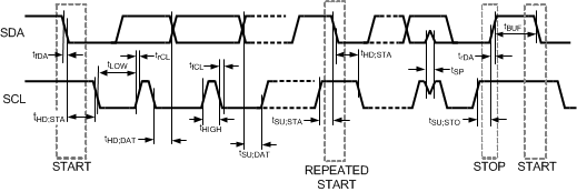 Figure 1. I2C Timing
6.10 Typical Characteristics
Unless otherwise specified: VVDDA5V = VVINBXX = 3.7 V, VOUT = 1.1 V, TA = 25°C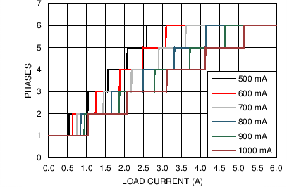
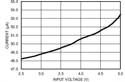
| VVIOSYS = 1.8 V | VNRST = 0 V |
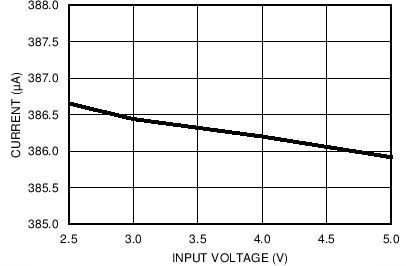
| PFM Mode | No load | One core active |
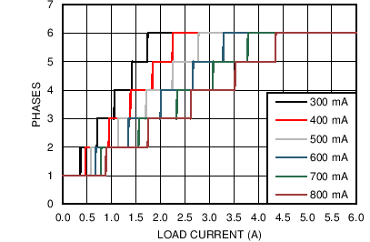
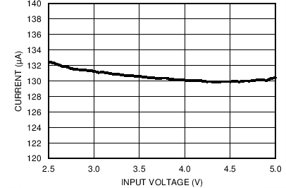
| Low-Power Mode | No load | One core active |
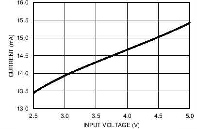
| PWM Mode | No load | One core active |