SNVSA06C March   2015  – August 2018 LP8758-B0

PRODUCTION DATA.  

  1. Features
  2. Applications
  3. Description
  4. Simplified Schematic
    1.     Efficiency vs Output Current (VIN = 3.7 V)
  5. Revision History
  6. Pin Configuration and Functions
    1.     Pin Functions
  7. Specifications
    1. 7.1 Absolute Maximum Ratings
    2. 7.2 ESD Ratings
    3. 7.3 Recommended Operating Conditions
    4. 7.4 Thermal Information
    5. 7.5 Electrical Characteristics
    6. 7.6 I2C Serial Bus Timing Parameter
    7. 7.7 Switching Characteristics
    8. 7.8 Typical Characteristics
  8. Detailed Description
    1. 8.1 Overview
      1. 8.1.1 Buck Information
        1. 8.1.1.1 Operating Modes
        2. 8.1.1.2 Features
        3. 8.1.1.3 Programmability
    2. 8.2 Functional Block Diagram
    3. 8.3 Feature Description
      1. 8.3.1 Multi-Phase DC-DC Converters
        1. 8.3.1.1 Overview
        2. 8.3.1.2 Multi-Phase Operation and Phase Adding/Shedding
        3. 8.3.1.3 Transition Between PWM and PFM Modes
        4. 8.3.1.4 Multi-Phase Switcher Configurations
        5. 8.3.1.5 Buck Converter Load Current Measurement
        6. 8.3.1.6 Spread-Spectrum Mode
      2. 8.3.2 Power-Up
      3. 8.3.3 Regulator Control
        1. 8.3.3.1 Enabling and Disabling Regulator
        2. 8.3.3.2 Changing Output Voltage
      4. 8.3.4 Device Reset Scenarios
      5. 8.3.5 Diagnosis and Protection Features
        1. 8.3.5.1 Warnings for Diagnosis (Interrupt)
          1. 8.3.5.1.1 Output Current Limit
          2. 8.3.5.1.2 Thermal Warning
        2. 8.3.5.2 Protection (Regulator Disable)
          1. 8.3.5.2.1 Short-Circuit and Overload Protection
          2. 8.3.5.2.2 Thermal Shutdown
        3. 8.3.5.3 Fault (Power Down)
          1. 8.3.5.3.1 Undervoltage Lockout
      6. 8.3.6 Digital Signal Filtering
    4. 8.4 Device Functional Modes
      1. 8.4.1 Modes of Operation
    5. 8.5 Programming
      1. 8.5.1 I2C-Compatible Interface
        1. 8.5.1.1 Data Validity
        2. 8.5.1.2 Start and Stop Conditions
        3. 8.5.1.3 Transferring Data
        4. 8.5.1.4 I2C-Compatible Chip Address
        5. 8.5.1.5 Auto Increment Feature
    6. 8.6 Register Maps
      1. 8.6.1 Register Descriptions
        1. 8.6.1.1  DEV_REV
        2. 8.6.1.2  OTP_REV
        3. 8.6.1.3  BUCK0_CTRL1
        4. 8.6.1.4  BUCK0_CTRL2
        5. 8.6.1.5  BUCK1_CTRL2
        6. 8.6.1.6  BUCK2_CTRL2
        7. 8.6.1.7  BUCK3_CTRL2
        8. 8.6.1.8  BUCK0_VOUT
        9. 8.6.1.9  BUCK0_FLOOR_VOUT
        10. 8.6.1.10 BUCK0_DELAY
        11. 8.6.1.11 RESET
        12. 8.6.1.12 CONFIG
        13. 8.6.1.13 INT_TOP
        14. 8.6.1.14 INT_BUCK_0_1
        15. 8.6.1.15 INT_BUCK_2_3
        16. 8.6.1.16 TOP_STAT
        17. 8.6.1.17 BUCK_0_1_STAT
        18. 8.6.1.18 BUCK_2_3_STAT
        19. 8.6.1.19 TOP_MASK
        20. 8.6.1.20 BUCK_0_1_MASK
        21. 8.6.1.21 BUCK_2_3_MASK
        22. 8.6.1.22 SEL_I_LOAD
        23. 8.6.1.23 I_LOAD_2
        24. 8.6.1.24 I_LOAD_1
  9. Application and Implementation
    1. 9.1 Application Information
    2. 9.2 Typical Application
      1. 9.2.1 Design Requirements
      2. 9.2.2 Detailed Design Procedure
        1. 9.2.2.1 Application Components
          1. 9.2.2.1.1 Inductor Selection
          2. 9.2.2.1.2 Input Capacitor Selection
          3. 9.2.2.1.3 Output Capacitor Selection
      3. 9.2.3 Application Curves
  10. 10Power Supply Recommendations
  11. 11Layout
    1. 11.1 Layout Guidelines
    2. 11.2 Layout Example
  12. 12Device and Documentation Support
    1. 12.1 Device Support
      1. 12.1.1 Third-Party Products Disclaimer
    2. 12.2 Documentation Support
      1. 12.2.1 Related Documentation
    3. 12.3 Receiving Notification of Documentation Updates
    4. 12.4 Community Resources
    5. 12.5 Trademarks
    6. 12.6 Electrostatic Discharge Caution
    7. 12.7 Glossary
  13. 13Mechanical, Packaging, and Orderable Information

Package Options

Mechanical Data (Package|Pins)
Thermal pad, mechanical data (Package|Pins)
Orderable Information

Changing Output Voltage

The regulator's output voltage can be changed by the ENx pin (voltage levels defined by the BUCK0_VOUT and BUCK0_FLOOR_VOUT registers) or by writing to the BUCK0_VOUT and BUCK0_FLOOR_VOUT registers. The voltage change is always slew-rate controlled, and the slew-rate is defined by the BUCKx_CTRL2.SLEW_RATE[2:0] bits. During voltage change the Forced PWM mode is used automatically. If the multi-phase operation is forced by the BUCK0_CTRL1. BUCK0_FPWM_MP bit, the regulator operates in multi-phase mode (four phases active). If the multi-phase operation is not forced, the number of phases are added and shedded automatically to follow the required slew rate. When the programmed output voltage is achieved, the mode becomes the one defined by load current, and the BUCK0_CTRL1.BUCK0_FPWM and BUCK0_CTRL1.BUCK0_FPWM_MP bits.
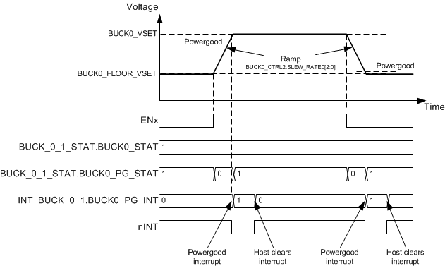
LP8758-B0 Voltage_Change_4ph.gifFigure 12. Regulator Output Voltage Change