SNVSC07A June 2021 – September 2022 LP876242-Q1
PRODUCTION DATA
- 1 Features
- 2 Applications
- 3 Description
- 4 Revision History
- 5 Pin Configuration and Functions
-
6 Specifications
- 6.1 Absolute Maximum Ratings
- 6.2 ESD Ratings
- 6.3 Recommended Operating Conditions
- 6.4 Thermal Information
- 6.5 Internal Low Drop-Out Regulators (LDOVINT)
- 6.6 BUCK1, BUCK2, BUCK3, and BUCK4 Regulators
- 6.7 Reference Generator (REFOUT)
- 6.8 Monitoring Functions
- 6.9 Clocks, Oscillators, and DPLL
- 6.10 Thermal Monitoring and Shutdown
- 6.11 System Control Thresholds
- 6.12 Current Consumption
- 6.13 Digital Input Signal Parameters
- 6.14 Digital Output Signal Parameters
- 6.15 I/O Pullup and Pulldown Resistance
- 6.16 I2C Interface
- 6.17 Serial Peripheral Interface (SPI)
- 25
- 6.18 Typical Characteristics
-
7 Detailed Description
- 7.1 Overview
- 7.2 Functional Block Diagram
- 7.3
Feature Description
- 7.3.1 Input Voltage Monitor
- 7.3.2 Power Resources
- 7.3.3 Residual Voltage Checking
- 7.3.4 Output Voltage Monitor and PGOOD Generation
- 7.3.5 General-Purpose I/Os (GPIO Pins)
- 7.3.6 Thermal Monitoring
- 7.3.7 Interrupts
- 7.3.8
Watchdog (WD)
- 7.3.8.1 Watchdog Fail Counter and Status
- 7.3.8.2 Watchdog Start-Up and Configuration
- 7.3.8.3 MCU to Watchdog Synchronization
- 7.3.8.4 Watchdog Disable Function
- 7.3.8.5 Watchdog Sequence
- 7.3.8.6 Watchdog Trigger Mode
- 7.3.8.7 WatchDog Flow Chart and Timing Diagrams in Trigger Mode
- 55
- 7.3.8.8 Watchdog Question-Answer Mode
- 7.3.9 Error Signal Monitor (ESM)
- 7.4
Device Functional Modes
- 7.4.1
Device State Machine
- 7.4.1.1 Fixed Device Power FSM
- 7.4.1.2
Pre-Configurable Mission States
- 7.4.1.2.1
PFSM Commands
- 7.4.1.2.1.1 REG_WRITE_IMM Command
- 7.4.1.2.1.2 REG_WRITE_MASK_IMM Command
- 7.4.1.2.1.3 REG_WRITE_MASK_PAGE0_IMM Command
- 7.4.1.2.1.4 REG_WRITE_BIT_PAGE0_IMM Command
- 7.4.1.2.1.5 REG_WRITE_WIN_PAGE0_IMM Command
- 7.4.1.2.1.6 REG_WRITE_VOUT_IMM Command
- 7.4.1.2.1.7 REG_WRITE_VCTRL_IMM Command
- 7.4.1.2.1.8 REG_WRITE_MASK_SREG Command
- 7.4.1.2.1.9 SREG_READ_REG Command
- 7.4.1.2.1.10 SREG_WRITE_IMM Command
- 7.4.1.2.1.11 WAIT Command
- 7.4.1.2.1.12 DELAY_IMM Command
- 7.4.1.2.1.13 DELAY_SREG Command
- 7.4.1.2.1.14 TRIG_SET Command
- 7.4.1.2.1.15 TRIG_MASK Command
- 7.4.1.2.1.16 END Command
- 7.4.1.2.2 Configuration Memory Organization and Sequence Execution
- 7.4.1.2.3 Mission State Configuration
- 7.4.1.2.4 Pre-Configured Hardware Transitions
- 7.4.1.2.1
PFSM Commands
- 7.4.1.3 Error Handling Operations
- 7.4.1.4 Device Start-up Timing
- 7.4.1.5 Power Sequences
- 7.4.1.6 First Supply Detection
- 7.4.2 Multi-PMIC Synchronization
- 7.4.1
Device State Machine
- 7.5 Control Interfaces
- 7.6 NVM Configurable Registers
- 7.7 Register Map
- 8 Application and Implementation
- 9 Device and Documentation Support
- 10Mechanical, Packaging, and Orderable Information
Package Options
Mechanical Data (Package|Pins)
- RQK|32
Thermal pad, mechanical data (Package|Pins)
Orderable Information
7.4.1.5 Power Sequences
A power sequence is an automatic preconfigured sequence the LP876242-Q1 device applies to its resources, which include the states of the BUCKs, the VMON1 and VMON2 and the GPIO output signals. For a detailed description of the GPIOs signals, please refer to General-Purpose I/Os (GPIO Pins).
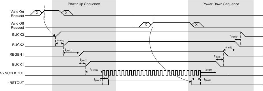
Figure 7-40 shows an example of a power up transition followed by a power down transition. The power up sequence is triggered through a valid on request, and the power down sequence is trigger by a valid off request. The resources controlled (for this example) are: BUCK3, BUCK2, REGEN1, SYNCCLKOUT, and nRSTOUT. The time between each resource enable and disable (TinstX) is also part of the preconfigured sequence definition.
A resource not assigned to any power sequence remains in off mode during the power-up sequence. The attached MCU or SoC can enable and configure this resource independently when the power-up sequence completes. Also the GPIO pin used as EN_DRV remains low during the power-up sequence. The attached MCU or SoC can release the EN_DRV pin by setting the ENABLE_DRV bit (requires running watchdog, ESM started and no pending interrupt bits).
 Figure 7-40 Power Sequence
Example
Figure 7-40 Power Sequence
ExampleAs the power sequences of the LP876242-Q1 device are defined according to the processor requirements, the total time for the completion of the power sequence varies across various system definitions.