SNVSC07A June 2021 – September 2022 LP876242-Q1
PRODUCTION DATA
- 1 Features
- 2 Applications
- 3 Description
- 4 Revision History
- 5 Pin Configuration and Functions
-
6 Specifications
- 6.1 Absolute Maximum Ratings
- 6.2 ESD Ratings
- 6.3 Recommended Operating Conditions
- 6.4 Thermal Information
- 6.5 Internal Low Drop-Out Regulators (LDOVINT)
- 6.6 BUCK1, BUCK2, BUCK3, and BUCK4 Regulators
- 6.7 Reference Generator (REFOUT)
- 6.8 Monitoring Functions
- 6.9 Clocks, Oscillators, and DPLL
- 6.10 Thermal Monitoring and Shutdown
- 6.11 System Control Thresholds
- 6.12 Current Consumption
- 6.13 Digital Input Signal Parameters
- 6.14 Digital Output Signal Parameters
- 6.15 I/O Pullup and Pulldown Resistance
- 6.16 I2C Interface
- 6.17 Serial Peripheral Interface (SPI)
- 25
- 6.18 Typical Characteristics
-
7 Detailed Description
- 7.1 Overview
- 7.2 Functional Block Diagram
- 7.3
Feature Description
- 7.3.1 Input Voltage Monitor
- 7.3.2 Power Resources
- 7.3.3 Residual Voltage Checking
- 7.3.4 Output Voltage Monitor and PGOOD Generation
- 7.3.5 General-Purpose I/Os (GPIO Pins)
- 7.3.6 Thermal Monitoring
- 7.3.7 Interrupts
- 7.3.8
Watchdog (WD)
- 7.3.8.1 Watchdog Fail Counter and Status
- 7.3.8.2 Watchdog Start-Up and Configuration
- 7.3.8.3 MCU to Watchdog Synchronization
- 7.3.8.4 Watchdog Disable Function
- 7.3.8.5 Watchdog Sequence
- 7.3.8.6 Watchdog Trigger Mode
- 7.3.8.7 WatchDog Flow Chart and Timing Diagrams in Trigger Mode
- 55
- 7.3.8.8 Watchdog Question-Answer Mode
- 7.3.9 Error Signal Monitor (ESM)
- 7.4
Device Functional Modes
- 7.4.1
Device State Machine
- 7.4.1.1 Fixed Device Power FSM
- 7.4.1.2
Pre-Configurable Mission States
- 7.4.1.2.1
PFSM Commands
- 7.4.1.2.1.1 REG_WRITE_IMM Command
- 7.4.1.2.1.2 REG_WRITE_MASK_IMM Command
- 7.4.1.2.1.3 REG_WRITE_MASK_PAGE0_IMM Command
- 7.4.1.2.1.4 REG_WRITE_BIT_PAGE0_IMM Command
- 7.4.1.2.1.5 REG_WRITE_WIN_PAGE0_IMM Command
- 7.4.1.2.1.6 REG_WRITE_VOUT_IMM Command
- 7.4.1.2.1.7 REG_WRITE_VCTRL_IMM Command
- 7.4.1.2.1.8 REG_WRITE_MASK_SREG Command
- 7.4.1.2.1.9 SREG_READ_REG Command
- 7.4.1.2.1.10 SREG_WRITE_IMM Command
- 7.4.1.2.1.11 WAIT Command
- 7.4.1.2.1.12 DELAY_IMM Command
- 7.4.1.2.1.13 DELAY_SREG Command
- 7.4.1.2.1.14 TRIG_SET Command
- 7.4.1.2.1.15 TRIG_MASK Command
- 7.4.1.2.1.16 END Command
- 7.4.1.2.2 Configuration Memory Organization and Sequence Execution
- 7.4.1.2.3 Mission State Configuration
- 7.4.1.2.4 Pre-Configured Hardware Transitions
- 7.4.1.2.1
PFSM Commands
- 7.4.1.3 Error Handling Operations
- 7.4.1.4 Device Start-up Timing
- 7.4.1.5 Power Sequences
- 7.4.1.6 First Supply Detection
- 7.4.2 Multi-PMIC Synchronization
- 7.4.1
Device State Machine
- 7.5 Control Interfaces
- 7.6 NVM Configurable Registers
- 7.7 Register Map
- 8 Application and Implementation
- 9 Device and Documentation Support
- 10Mechanical, Packaging, and Orderable Information
Package Options
Mechanical Data (Package|Pins)
- RQK|32
Thermal pad, mechanical data (Package|Pins)
Orderable Information
7.3.2.1.5 Sync Clock Functionality
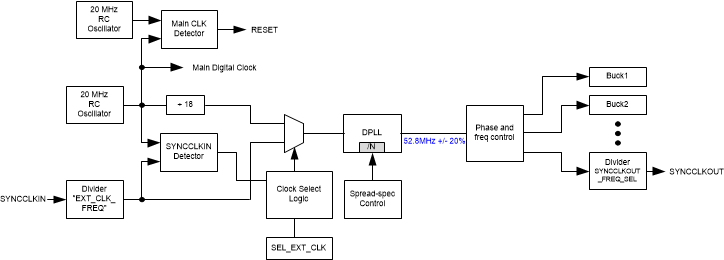
The LP876242-Q1 device contains a SYNCCLKIN input to synchronize switching clock of the buck regulator with the external clock. The block diagram of the clocking and DPLL module is shown in Figure 7-7. The external clock is selected when the external clock is available, and SEL_EXT_CLK = '1'. The nominal frequency of the external input clock is set by EXT_CLK_FREQ[1:0] bits in the NVM and it can be 1.1 MHz, 2.2 MHz, 4.4 MHz, or 8.8 MHz.
The EXT_CLK_INT interrupt is also generated in cases the external clock is expected, but it is not available.
The LP876242-Q1 device can also generate clock SYNCCLKOUT for external device use. The SYNCCLKOUT_FREQ_SEL[1:0] selects the frequency of the SYNCCLKOUT. Please note that SYNCCLKOUT_FREQ_SEL[1:0] must stay static while SYNCCLKOUT is used, as changing the output frequency selection may cause glitches on the clock output.
 Figure 7-7 Sync
Clock and DPLL Module