SNVSBD3B August 2020 – May 2024 LP8864S-Q1
PRODUCTION DATA
- 1
- 1 Features
- 2 Applications
- 3 Description
- 4 Pin Configuration and Functions
- 5 Specifications
-
6 Detailed Description
- 6.1 Overview
- 6.2 Functional Block Diagram
- 6.3
Feature Description
- 6.3.1 Control Interface
- 6.3.2 Function Setting
- 6.3.3 Device Supply (VDD)
- 6.3.4 Enable (EN)
- 6.3.5 Charge Pump
- 6.3.6 Boost Controller
- 6.3.7 LED Current Sinks
- 6.3.8 Brightness Control
- 6.3.9
Protection and Fault Detections
- 6.3.9.1 Supply Faults
- 6.3.9.2
Boost Faults
- 6.3.9.2.1 Boost Overvoltage Faults (BSTOVPL, BSTOVPH)
- 6.3.9.2.2 Boost Overcurrent Faults (BSTOCP)
- 6.3.9.2.3 LEDSET Resistor Missing Faults (LEDSET)
- 6.3.9.2.4 MODE Resistor Missing Faults (MODESEL)
- 6.3.9.2.5 FSET Resistor Missing Faults (FSET)
- 6.3.9.2.6 ISET Resistor Out of Range Faults (ISET)
- 6.3.9.2.7 Thermal Shutdown Faults (TSD)
- 6.3.9.3 LED Faults
- 6.3.9.4 Overview of the Fault and Protection Schemes
- 6.4 Device Functional Modes
- 6.5 Programming
- 7 Register Maps
-
8 Application and Implementation
- 8.1 Application Information
- 8.2
Typical Applications
- 8.2.1
Full Feature Application for Display Backlight
- 8.2.1.1 Design Requirements
- 8.2.1.2
Detailed Design Procedure
- 8.2.1.2.1 Inductor Selection
- 8.2.1.2.2 Output Capacitor Selection
- 8.2.1.2.3 Input Capacitor Selection
- 8.2.1.2.4 Charge Pump Output Capacitor
- 8.2.1.2.5 Charge Pump Flying Capacitor
- 8.2.1.2.6 Output Diode
- 8.2.1.2.7 Switching FET
- 8.2.1.2.8 Boost Sense Resistor
- 8.2.1.2.9 Power-Line FET
- 8.2.1.2.10 Input Current Sense Resistor
- 8.2.1.2.11 Feedback Resistor Divider
- 8.2.1.2.12 Critical Components for Design
- 8.2.1.3 Application Curves
- 8.2.2 Application with Basic/Minimal Operation
- 8.2.3
SEPIC Mode Application
- 8.2.3.1 Design Requirements
- 8.2.3.2
Detailed Design Procedure
- 8.2.3.2.1 Inductor Selection
- 8.2.3.2.2 Coupling Capacitor Selection
- 8.2.3.2.3 Output Capacitor Selection
- 8.2.3.2.4 Input Capacitor Selection
- 8.2.3.2.5 Charge Pump Output Capacitor
- 8.2.3.2.6 Charge Pump Flying Capacitor
- 8.2.3.2.7 Switching FET
- 8.2.3.2.8 Output Diode
- 8.2.3.2.9 Switching Sense Resistor
- 8.2.3.2.10 Power-Line FET
- 8.2.3.2.11 Input Current Sense Resistor
- 8.2.3.2.12 Feedback Resistor Divider
- 8.2.3.2.13 Critical Components for Design
- 8.2.3.3 Application Curves
- 8.2.1
Full Feature Application for Display Backlight
- 8.3 Power Supply Recommendations
- 8.4 Layout
- 9 Device and Documentation Support
- 10Revision History
- 11Mechanical, Packaging, and Orderable Information
Package Options
Mechanical Data (Package|Pins)
Thermal pad, mechanical data (Package|Pins)
Orderable Information
6.3.9.1.1 VIN Undervoltage Faults (VINUVLO)
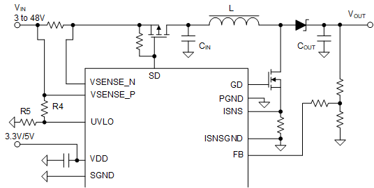
The LP8864S-Q1 device supports VIN undervoltage and overvoltage protection. The undervoltage threshold is programmable through external resistor divider on UVLO pin. If during operation of the LP8864S-Q1 device, the UVLO pin voltage falls below the UVLO falling level (0.787V typical), the boost, LED outputs, and power-line FET will be turned off, and the device will enter STANDBY mode. The VINUVLO_STATUS bit is also set in the SUPPLY_FAULT_STATUS register, and the INT pin is triggered. When the UVLO voltage rises above the rising threshold level the LP8864S-Q1 exits STANDBY and begins the start-up sequence.
 Figure 6-16 VIN UVLO Setting
Circuit
Figure 6-16 VIN UVLO Setting
CircuitThe following equation is used to calculate the UVLO threshold for VIN rising edge:

where
- VINUVLO_TH = 0.787V
The hysteresis of UVLO threshold can be designed and calculated with the following equation.

where
- IUVLO = 5µA
So the following equation can be used for UVLO threshold for VIN falling edge:

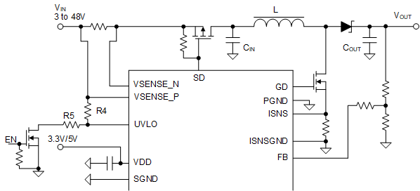
The bottom resistors, R5 of voltage divider is able to be disconnected to the GND through an additional external N-type of FET as Figure 6-17. This design is to minimize the current leakage from VIN in shutdown mode to extend the battery life.
 Figure 6-17 VIN UVLO Setting Circuit Without Current Leakage Path