SNOS413E August 2000 – November 2016 LPV321-N , LPV324-N , LPV358-N
PRODUCTION DATA.
- 1 Features
- 2 Applications
- 3 Description
- 4 Revision History
- 5 Pin Configuration and Functions
- 6 Specifications
- 7 Detailed Description
- 8 Application and Implementation
- 9 Power Supply Recommendations
- 10Layout
- 11Device and Documentation Support
- 12Mechanical, Packaging, and Orderable Information
Package Options
Mechanical Data (Package|Pins)
Thermal pad, mechanical data (Package|Pins)
Orderable Information
8 Application and Implementation
NOTE
Information in the following applications sections is not part of the TI component specification, and TI does not warrant its accuracy or completeness. TI’s customers are responsible for determining suitability of components for their purposes. Customers should validate and test their design implementation to confirm system functionality.
8.1 Application Information
The LPV3xx-N family of amplifiers is specified for operation from 2.7 V to 5 V (±1.35 V to ±2.5 V). Many of the specifications apply from –40°C to 125°C. They provide ground-sensing inputs as well as rail-to-rail output swing. Parameters that can exhibit significant variance with regard to operating voltage or temperature are presented in the Typical Characteristics.
8.2 Typical Applications
8.2.1 Simple Low-Pass Active Filter
A simple low-pass filter is shown in Figure 41.
 Figure 41. Simple Low-Pass Active Filter Schematic
8.2.1.1 Design Requirements
The low-pass filter is shown in Figure 41 passes low frequencies and attenuate frequencies above corner frequency (fc) at a roll-off rate of 20 dB/Decade.
8.2.1.2 Detailed Design Procedure
The low-frequency gain (ω → o) is defined by −R3/R1. This allows low-frequency gains other than unity to be obtained. The filter has a −20 dB/decade roll-off after its corner frequency fc. R2 must be chosen equal to the parallel combination of R1 and R3 to minimize errors due to bais current. The frequency response of the filter is shown in Figure 42.

Note that the single op amp active filters are used in to the applications that require low quality factor, Q (≤ 10), low frequency (≤ 5 kHz), and low gain (≤ 10), or a small value for the product of gain times Q (≤ 100). The op amp must have an open loop voltage gain at the highest frequency of interest at least 50 times larger than the gain of the filter at this frequency. In addition, the selected op amp must have a slew rate that meets the requirements in Equation 2.
where
- ωH is the highest frequency of interest
- VOPP is the output peak-to-peak voltage
8.2.1.3 Application Curve
 Figure 42. Frequency Response of Simple Low-pass Active Filter
8.2.2 Difference Amplifier
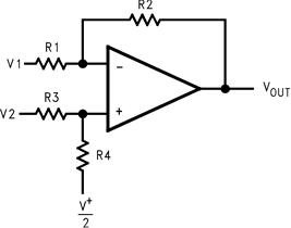
The difference amplifier allows the subtraction of two voltages or, as a special case, the cancellation of a signal common to two inputs. It is useful as a computational amplifier in making a differential to single-ended conversion or in rejecting a common mode signal.
 Figure 43. Difference Amplifier Schematic

8.2.3 Instrumentation Circuits
The input impedance of the previous difference amplifier is set by the resistor R1, R2, R3, and R4. To eliminate the problems of low input impedance, one way is to use a voltage follower ahead of each input as shown in the following two instrumentation amplifiers.
8.2.3.1 Three Operating Amplifier Instrumentation
The quad LPV324 can be used to build a three-op-amp instrumentation amplifier as shown in Figure 44
 Figure 44. Three-op-amp Instrumentation Amplifier Schematic
The first stage of this instrumentation amplifier is a differential-input, differential-output amplifier, with two voltage followers. These two voltage followers assure that the input impedance is over 100 MΩ. The gain of this instrumentation amplifier is set by the ratio of R2/R1. R3 should equal R1 and R4 equal R2. Matching of R3 to R1 and R4 to R2 affects the CMRR. For good CMRR over temperature, low drift resistors should be used. Making R4 Slightly smaller than R 2 and adding a trim pot equal to twice the difference between R 2 and R4 will allow the CMRR to be adjusted for optimum.
8.2.3.2 Two Operating Amplifier Instrumentation
A two-op-amp instrumentation amplifier can also be used to make a high-input-impedance DC differential amplifier (Figure 45). As in the three-op-amp circuit, this instrumentation amplifier requires precise resistor matching for good CMRR. R4 should equal to R1 and R3 must equal R2.
 Figure 45. Two-op-amp Instrumentation Amplifier Schematic

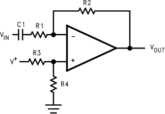
8.2.3.3 Single-Supply Inverting Amplifier
There may be cases where the input signal going into the amplifier is negative. Because the amplifier is operating in single supply voltage, a voltage divider using R3 and R4 is implemented to bias the amplifier so the input signal is within the input common-common voltage range of the amplifier. The capacitor C1 is placed between the inverting input and resistor R1 to block the DC signal going into the AC signal source, VIN. The values of R1 and C1 affect the cutoff frequency in Equation 5.
As a result, the output signal is centered around mid-supply (if the voltage divider provides V+/2 at the non-inverting input). The output can swing to both rails, maximizing the signal-to-noise ratio in a low voltage system.
 Figure 46. Single-Supply Inverting Amplifier
