SNVSA49B january   2015  – june 2023 LV2862

PRODUCTION DATA  

  1.   1
  2. Features
  3. Applications
  4. Description
  5. Revision History
  6. Pin Configuration and Functions
  7. Specifications
    1. 6.1 Absolute Maximum Ratings
    2. 6.2 ESD Ratings
    3. 6.3 Recommended Operating Conditions
    4. 6.4 Thermal Information
    5. 6.5 Electrical Characteristics
    6. 6.6 Typical Characteristics
  8. Detailed Description
    1. 7.1 Overview
    2. 7.2 Functional Block Diagram
    3. 7.3 Feature Description
      1. 7.3.1 Continuous Conduction Mode
      2. 7.3.2 Fixed Frequency PWM Control
      3. 7.3.3 Eco-mode
      4. 7.3.4 Bootstrap Voltage (CB)
      5. 7.3.5 Enable (SHDN) and VIN Undervoltage Lockout (UVLO)
      6. 7.3.6 Setting the Output Voltage
      7. 7.3.7 Current Limit
      8. 7.3.8 Thermal Shutdown
    4. 7.4 Device Functional Modes
  9. Application and Implementation
    1. 8.1 Application Information
    2. 8.2 Typical Application
      1. 8.2.1 Design Requirements
        1. 8.2.1.1 Design Guide – Step By Step Design Procedure
      2. 8.2.2 Detailed Design Procedure
        1. 8.2.2.1 Selecting the Switching Frequency
        2. 8.2.2.2 Output Inductor Selection
        3. 8.2.2.3 Output Capacitor Selection
        4. 8.2.2.4 Schottky Diode Selection
        5. 8.2.2.5 Input Capacitor Selection
          1. 8.2.2.5.1 Bootstrap Capacitor Selection
            1. 8.2.2.5.1.1 Typical Application Circuits
      3. 8.2.3 Application Curves
    3. 8.3 Power Supply Recommendations
    4. 8.4 Layout
      1. 8.4.1 Layout Guidelines
      2. 8.4.2 Layout Example
  10. Device and Documentation Support
    1. 9.1 Documentation Support
      1. 9.1.1 Related Documentation
    2. 9.2 Receiving Notification of Documentation Updates
    3. 9.3 Support Resources
    4. 9.4 Trademarks
    5. 9.5 Electrostatic Discharge Caution
    6. 9.6 Glossary
  11. 10Mechanical, Packaging, and Orderable Information

Package Options

Mechanical Data (Package|Pins)
Thermal pad, mechanical data (Package|Pins)
Orderable Information

Description

The LV2862 is a PWM DC/DC buck (step-down) regulator. With a wide input range from 4 V to 60 V, the device is designed for a wide range of applications, from industrial to automotive, for power conditioning from unregulated source. An ultra-low 1-µA shutdown current can further prolong battery life. Operating frequency is fixed at 770 kHz (X version) and 2.1 MHz (Y version), allowing the use of small external components while still being able to have low output ripple voltage. Soft start and compensation circuits are implemented internally, which allows the device to be used with minimized external components.

The LV2862 is optimized for up to 600-mA load currents. The device has a 0.765-V nominal feedback voltage.

The device has built-in protection features such as pulse-by-pulse current limit, thermal sensing, and shutdown due to excessive power dissipation. The LV2862 is available in a low profile SOT-6L package.

Package Information
PART NUMBER PACKAGE(1) PACKAGE SIZE(2)
LV2862 DDC (SOT, 6) 2.90 mm × 2.8 mm
For all available packages, see the orderable addendum at the end of the data sheet.
The package size (length × width) is a nominal value and includes pins, where applicable.
GUID-59E1E2D9-7CB5-4E2C-A92C-B3DB88810573-low.svgSimplified Schematic
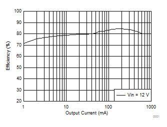
GUID-EDC1A1FA-43E8-4523-9A0D-7136B4CC79A8-low.gifEfficiency versus Output Current
(fsw = 0.7 MHz, VOUT = 3.3 V)