SNVSA49B january   2015  – june 2023 LV2862

PRODUCTION DATA  

  1.   1
  2. Features
  3. Applications
  4. Description
  5. Revision History
  6. Pin Configuration and Functions
  7. Specifications
    1. 6.1 Absolute Maximum Ratings
    2. 6.2 ESD Ratings
    3. 6.3 Recommended Operating Conditions
    4. 6.4 Thermal Information
    5. 6.5 Electrical Characteristics
    6. 6.6 Typical Characteristics
  8. Detailed Description
    1. 7.1 Overview
    2. 7.2 Functional Block Diagram
    3. 7.3 Feature Description
      1. 7.3.1 Continuous Conduction Mode
      2. 7.3.2 Fixed Frequency PWM Control
      3. 7.3.3 Eco-mode
      4. 7.3.4 Bootstrap Voltage (CB)
      5. 7.3.5 Enable (SHDN) and VIN Undervoltage Lockout (UVLO)
      6. 7.3.6 Setting the Output Voltage
      7. 7.3.7 Current Limit
      8. 7.3.8 Thermal Shutdown
    4. 7.4 Device Functional Modes
  9. Application and Implementation
    1. 8.1 Application Information
    2. 8.2 Typical Application
      1. 8.2.1 Design Requirements
        1. 8.2.1.1 Design Guide – Step By Step Design Procedure
      2. 8.2.2 Detailed Design Procedure
        1. 8.2.2.1 Selecting the Switching Frequency
        2. 8.2.2.2 Output Inductor Selection
        3. 8.2.2.3 Output Capacitor Selection
        4. 8.2.2.4 Schottky Diode Selection
        5. 8.2.2.5 Input Capacitor Selection
          1. 8.2.2.5.1 Bootstrap Capacitor Selection
            1. 8.2.2.5.1.1 Typical Application Circuits
      3. 8.2.3 Application Curves
    3. 8.3 Power Supply Recommendations
    4. 8.4 Layout
      1. 8.4.1 Layout Guidelines
      2. 8.4.2 Layout Example
  10. Device and Documentation Support
    1. 9.1 Documentation Support
      1. 9.1.1 Related Documentation
    2. 9.2 Receiving Notification of Documentation Updates
    3. 9.3 Support Resources
    4. 9.4 Trademarks
    5. 9.5 Electrostatic Discharge Caution
    6. 9.6 Glossary
  11. 10Mechanical, Packaging, and Orderable Information

Package Options

Mechanical Data (Package|Pins)
Thermal pad, mechanical data (Package|Pins)
Orderable Information

Pin Configuration and Functions

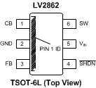
GUID-E14CFD44-3664-4DCC-8B2A-CBF2052F4246-low.gif Figure 5-1 SOT (DDC)6 PinsTop View
Table 5-1 Pin Functions
PIN DESCRIPTION
NAME NO.
CB 1 Switch FET gate bias voltage. Connect Cboot cap between CB and SW.
GND 2 Ground connection
FB 3 Set feedback voltage divider ratio with VOUT = VFB (1 + (R1 / R2))
SHDN 4 Enable and disable input (high voltage tolerant). Internal pullup current source. Pull below 1.25 V to disable. Float to enable. Establish the input undervoltage lockout with a two-resistor divider.
VIN 5 Power input voltage pin. Input for internal supply and drain node input for internal high-side MOSFET.
SW 6 Switch node. Connect to inductor, diode, and Cboot cap.