SLUSDA9C may   2018  – august 2023 LV3842

PRODUCTION DATA  

  1.   1
  2. Features
  3. Applications
  4. Description
  5. Revision History
  6. Device Comparison Table
  7. Pin Configuration and Functions
  8. Specifications
    1. 7.1 Absolute Maximum Ratings
    2. 7.2 ESD Ratings
    3. 7.3 Recommended Operating Conditions
    4. 7.4 Thermal Information
    5. 7.5 Electrical Characteristics
    6. 7.6 Timing Requirements
    7. 7.7 Switching Characteristics
    8. 7.8 Typical Characteristics
  9. Detailed Description
    1. 8.1 Overview
    2. 8.2 Functional Block Diagram
    3. 8.3 Feature Description
      1. 8.3.1 Fixed Frequency Peak Current Mode Control
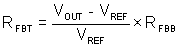
      2. 8.3.2 Adjustable Output Voltage
      3. 8.3.3 Enable
      4. 8.3.4 Minimum ON-Time, Minimum OFF-Time and Frequency Foldback
      5. 8.3.5 Bootstrap Voltage
      6. 8.3.6 Overcurrent and Short-Circuit Protection
      7. 8.3.7 Soft Start
      8. 8.3.8 Thermal Shutdown
    4. 8.4 Device Functional Modes
      1. 8.4.1 Shutdown Mode
      2. 8.4.2 Active Mode
      3. 8.4.3 CCM Mode
      4. 8.4.4 Light-Load Operation (PFM Version)
      5. 8.4.5 Light-Load Operation (FPWM Version)
  10. Application and Implementation
    1. 9.1 Application Information
    2. 9.2 Typical Application
      1. 9.2.1 Design Requirements
      2. 9.2.2 Detailed Design Procedure
        1. 9.2.2.1 Output Voltage Set-Point
        2. 9.2.2.2 Inductor Selection
        3. 9.2.2.3 Output Capacitor Selection
        4. 9.2.2.4 Input Capacitor Selection
        5. 9.2.2.5 Bootstrap Capacitor
        6. 9.2.2.6 Undervoltage Lockout Set-Point
      3. 9.2.3 Application Curves
    3. 9.3 Power Supply Recommendations
    4. 9.4 Layout
      1. 9.4.1 Layout Guidelines
      2. 9.4.2 Compact Layout for EMI Reduction
      3. 9.4.3 Feedback Resistors
      4. 9.4.4 Layout Example
  11. 10Device and Documentation Support
    1. 10.1 Documentation Support
      1. 10.1.1 Related Documentation
    2. 10.2 Receiving Notification of Documentation Updates
    3. 10.3 Support Resources
    4. 10.4 Trademarks
    5. 10.5 Electrostatic Discharge Caution
    6. 10.6 Glossary
  12. 11Mechanical, Packaging, and Orderable Information

Package Options

Mechanical Data (Package|Pins)
Thermal pad, mechanical data (Package|Pins)
Orderable Information

Adjustable Output Voltage

A precision 1.0-V reference voltage VREF is used to maintain a tightly regulated output voltage over the entire operating temperature range. The output voltage is set by a resistor divider from output voltage to the FB pin. TI recommends to use 1% tolerance resistors with a low temperature coefficient for the FB divider. Select the bottom-side resistor RFBB for the desired divider current and use Equation 1 to calculate top-side resistor RFBT. TI recommends RFBT in the range from 10 kΩ to 100 kΩ for most applications. Lower RFBT reduces efficiency at very light load. Less static current goes through a larger RFBT and can be more desirable when light-load efficiency is critical. But TI does not recommend RFBT larger than 1 MΩ because it makes the feedback path more susceptible to noise. Larger RFBT value requires more carefully designed feedback path on the PCB. The tolerance and temperature variation of the resistor dividers affect the output voltage regulation.

GUID-31993241-E7E2-4D1A-814C-C6128BE17EBE-low.gifFigure 8-2 Output Voltage Setting
Equation 1. GUID-C842C7DA-006A-48E0-AB22-87314F63C7C6-low.gif